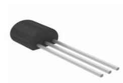
Transistors - JFETs JFET N-CH 25V 625MW TO92
J108 is a JFET N-Channel transistor. This article covers its datasheet, pinout, feature and more details about J108. Welcome your RFQ!

Transistors - JFETs JFET N-CH 25V 625MW TO92 J108 is a JFET N-Channel transistor. This article covers its datasheet, pinout, feature and more details about J108. Welcome your RFQ!
41
Nov 25, 2021
Blithe Chapman
Transistors - JFETs JFET N-CH 25V 625MW TO92
J108 is a JFET N-Channel transistor. This article covers its datasheet, pinout, feature and more details about J108. Welcome your RFQ!
J108
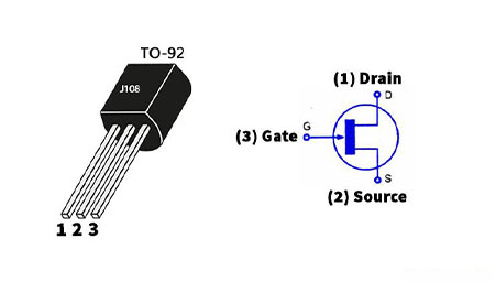
J108 Pinout
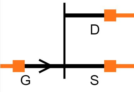
J108 Symbol

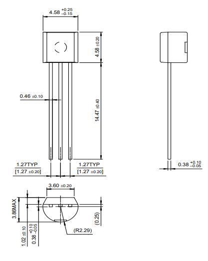
J108 Footprint
J108 JFET N-Channel Transistor is designed for analogue or digital switching applications where very low on-resistance is mandatory.
Type Designator: J108
Type of Transistor: JFET
Type of Control Channel: N-Channel
Package: TO-92
High-speed switching.
Interchangeability of drain and source connections.
Analogue switches
Choppers and commutators
Audio amplifiers
The equivalent for J108:
J105
J106
J107
J109
ON Semiconductor J108 technical specifications, attributes, parameters and parts with similar specifications to ON Semiconductor J108.
ON Semiconductor J108 technical specifications, attributes, parameters and parts with similar specifications to ON Semiconductor J108.
| Product Attribute | Attribute Value | |
|---|---|---|
| Mount | Through Hole | |
| Mounting Type | Through Hole | |
| Package / Case | TO-226-3, TO-92-3 (TO-226AA) | |
| Number of Pins | 3Pins | |
| Supplier Device Package | TO-92-3 | |
| Weight | 201mg | |
| Breakdown Voltage / V | -25V | |
| Operating Temperature | -55°C~150°C TJ | |
| Packaging | Bulk | |
| Part Status | Obsolete | |
| Moisture Sensitivity Level (MSL) | 1 (Unlimited) | |
| Termination | Through Hole |
| Product Attribute | Attribute Value | |
|---|---|---|
| Max Operating Temperature | 150°C | |
| Min Operating Temperature | -55°C | |
| Voltage - Rated DC | 25V | |
| Max Power Dissipation | 625mW | |
| Current Rating | 80mA | |
| Base Part Number | J108 | |
| Element Configuration | Single | |
| Power Dissipation | 625mW | |
| Output Power | 625mW | |
| Power - Max | 625mW | |
| FET Type | N-Channel | |
| Drain to Source Voltage (Vdss) | 25V |
| Product Attribute | Attribute Value | |
|---|---|---|
| Continuous Drain Current (ID) | 80mA | |
| Gate to Source Voltage (Vgs) | 25V | |
| Drain to Source Resistance | 8Ohm | |
| Current - Drain (Idss) @ Vds (Vgs=0) | 80mA @ 15V | |
| Voltage - Cutoff (VGS off) @ Id | 3V @ 10nA | |
| Voltage - Breakdown (V(BR)GSS) | 25V | |
| Resistance - RDS(On) | 8Ohms | |
| REACH SVHC | No SVHC | |
| RoHS Status | RoHS Compliant | |
| Lead Free | Lead Free |
ON Semiconductor (Nasdaq: ON) is driving energy efficient innovations, empowering customers to reduce global energy use. The company offers a comprehensive portfolio of energy-efficient power and signal management, logic, discrete and custom solutions to help design engineers solve their unique design challenges in automotive, communications, computing, consumer, industrial, LED lighting, medical, military/aerospace and power supply applications.
ON Semiconductor operates a responsive, reliable, world-class supply chain and quality program, and a network of manufacturing facilities, sales offices and design centres in key markets throughout North America, Europe, and the Asia Pacific regions.
Download datasheets and manufacturer documentation for J108
TAGS
Comments