ATTENTION: Due to increased demand and order volume, processing time may take an additional 1-3 business days.
HomeCommunitySubjectJ111 JFET Transistor: J111 Datasheet, Pinout, Equivalent

J111 JFET Transistor: J111 Datasheet, Pinout, Equivalent

J111 JFET N Channel Transistor is designed for low-level analogue switching, sample and hold circuits and chopper stabilized amplifiers. This article will unlock its datasheet, pinout, equivalent, application, and more detailed information about J111.

2529

Apr 13, 2022

Fanny Stuart

Construction and Working of JFET


J111 JFET N Channel Transistor is designed for low-level analogue switching, sample and hold circuits and chopper stabilized amplifiers. This article will unlock its datasheet, pinout, equivalent, application, and more detailed information about J111.


J111

9000In Stock
Min.: 1 Mult.: 1
Quantity Unit Price Ext. Price
1+ $0.3701$0.37
10+ $0.34915$3.49
100+ $0.32938$32.94
500+ $0.31074$155.37
1000+ $0.29315$293.15
Unit Price:$0.3701
Subtotal: $0.37
Looking for a better price? Want a lower wholesale price? Please send an RFQ, and we will respond immediately.
Quick Links

J111 Pinout

J111 Pinout

J111 CAD Model

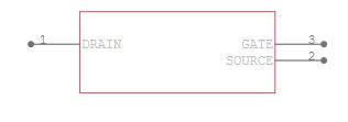
Symbol

J111 Symbol

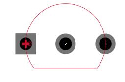
Footprint

J111 Footprint

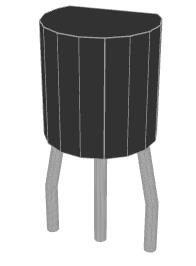
3D Model

J111 3D Model


J111 Description

J111 is a silicon field-effect transistor with an N channel that is available in TO-92  and SOT-23 packagesJ111  is a transistor in the J11x series, which also includes J112  and J113  transistors. All transistors in this series are designed primarily for analogue switching, current limiting, choppers, commentators, and sample and hold applications.

There are numerous advantages to incorporating these transistors in your design, including improved frequency response, high precision, reduced insertion loss, and low cost. Furthermore, the transistor has a low noise feature, allowing it to be employed in applications where the user has low noise requirements. The transistor also possesses symmetrical properties, which implies that the transistor's drain and source can be interchanged.

J111 Feature

  • TO-92 and SOT-23 packages are available.

  • N Channel JFET is a type of transistor (Symmetrical)

  • 35V is the maximum drain-to-gate voltage.

  • –35V is the maximum reverse gate to source voltage.

  • 50mA is the maximum continue gate current.

  • –5 to –3V is the maximum gate-to-source cutoff voltage.

  • 625mW is the maximum power dissipation.

  • The maximum storage and operating temperatures should be between -55  and +150 °C.

J111 Application

  • Analog Switches

  • Choppers

  • Sample-and-Hold

  • Normally “On” Switches

  • Current Limiters

How to Use J111?

As previously stated, the J111 FET  or field-effect transistor is generally intended for current limiting, analogue switching, choppers, commentators, and sample and hold applications; nevertheless, the J111 transistor is a versatile device that may be utilized in a wide range of applications. The J111 is a good choice if you require a fast switching transistor with minimal leakage and capacitance.

How to Operate J111 in Safety?

It is usually suggested to check the absolute maximum ratings of the transistor before using it in your design or circuit, and we also propose that you do not utilize a component on its absolute maximum ratings, but rather remain at least 20% below them. As a result, the same holds true for the J111 transistor. Because the maximum drain to gate voltage is 35V, do not drive loads greater than 28V. Because the maximum continuous gate current is 50mA, do not drive a load more than 40mA and always store or operate the transistor at temperatures greater than -55°C and less than +150 °C.


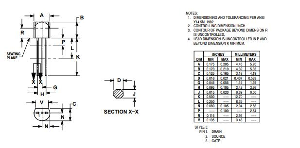
J111 Package

J111 Package

J111 Manufacturer

ON Semiconductor (Nasdaq: ON) is driving energy efficient innovations, empowering customers to reduce global energy use. The company offers a comprehensive portfolio of energy-efficient power and signal management, logic, discrete and custom solutions to help design engineers solve their unique design challenges in automotive, communications, computing, consumer, industrial, LED lighting, medical, military/aerospace and power supply applications.  ON Semiconductor operates a responsive, reliable, world-class supply chain and quality program, and a network of manufacturing facilities, sales offices and design centres in key markets throughout North America, Europe, and the Asia Pacific regions.

Specifications

ON Semiconductor J111 technical specifications, attributes, parameters and parts with similar specifications to ON Semiconductor J111.

J111 Tech Specifications

ON Semiconductor J111 technical specifications, attributes, parameters and parts with similar specifications to ON Semiconductor J111.

Product Attribute Attribute Value
Lifecycle StatusACTIVE (Last Updated: 20 hours ago)
Factory Lead Time6 Weeks
MountThrough Hole
Mounting TypeThrough Hole
Package / CaseTO-226-3, TO-92-3 (TO-226AA)
Number of Pins3Pins
Supplier Device PackageTO-92-3
Weight201mg
Manufacturer Package IdentifierTO-92 3L
Breakdown Voltage / V-35V
Operating Temperature-55°C~150°C TJ
PackagingBulk
Published2006
Part StatusActive
Product Attribute Attribute Value
Moisture Sensitivity Level (MSL)1 (Unlimited)
TerminationThrough Hole
Max Operating Temperature150°C
Min Operating Temperature-55°C
Voltage - Rated DC35V
Max Power Dissipation625mW
Current Rating50mA
Base Part NumberJ111
Element ConfigurationSingle
Power Dissipation625mW
Power - Max625mW
FET TypeN-Channel
Drain to Source Voltage (Vdss)35V
Continuous Drain Current (ID)20mA
Product Attribute Attribute Value
Gate to Source Voltage (Vgs)-35V
Drain to Source Resistance30Ohm
Current - Drain (Idss) @ Vds (Vgs=0)20mA @ 15V
Voltage - Cutoff (VGS off) @ Id3V @ 1μA
Voltage - Breakdown (V(BR)GSS)35V
Resistance - RDS(On)30Ohms
Height5.33mm
Length5.2mm
Width4.19mm
REACH SVHCNo SVHC
Radiation HardeningNo
RoHS StatusROHS3 Compliant
Lead FreeLead Free
0 Products View Similar

Datasheet PDF

J111 Documents

Download datasheets and manufacturer documentation for J111

Frequently Asked Questions

What channel does J111 have?
J111 is a silicon field-effect transistor with an N channel.
What types of transistors are included in the J11x series?
J111, J112 and J113.
What feature does J111 have?
Low noise feature.
How much below the absolute maximum ratings of the J111 transistor?
20%.
What type of transistor does the same hold true for?
J111.
FAQ
What channel does J111 have?
J111 is a silicon field-effect transistor with an N channel.
What types of transistors are included in the J11x series?
J111, J112 and J113.
What feature does J111 have?
Low noise feature.
How much below the absolute maximum ratings of the J111 transistor?
20%.
What type of transistor does the same hold true for?
J111.

TAGS

Share