ATTENTION: Due to increased demand and order volume, processing time may take an additional 1-3 business days.
HomeCommunitySubjectJ113 N-Channel Switch: J113 Transistor Equivalents and Datasheet

J113 N-Channel Switch: J113 Transistor Equivalents and Datasheet

JFET N-CH 35V 625MW TO92 J113 is a J11x series N Channel silicon FET or field-effect transistor. J111 and J112 are two more transistors in this family. This article is going to cover datasheet, pinout, equivalents about J113 transistor.
3551

Mar 15, 2022

Darlene Kent

Mega 328 medida de jfet TESTER J201 2N5457 J112 J111 J113


JFET N-CH 35V 625MW TO92

J113 is a J11x series N Channel silicon FET or field-effect transistor. J111 and J112 are two more transistors in this family. This article is going to cover datasheet, pinout, equivalents about J113 transistor.
 

J113_D75Z

Inquiry
Min.: 1 Mult.: 1
Price not displayed? Not available to buy online? Please send an RFQ, and we will respond immediately.
Quick Links

What is J113?

J113 is a J11x series N Channel silicon FET  or field-effect transistor. J111  and J112  are two more transistors in this family. TO-92  and SOT-23 packaging are available for the transistors.

They're primarily employed in choppers, sample and hold applications, current limiting applications, switching applications, commentators, and other similar applications.

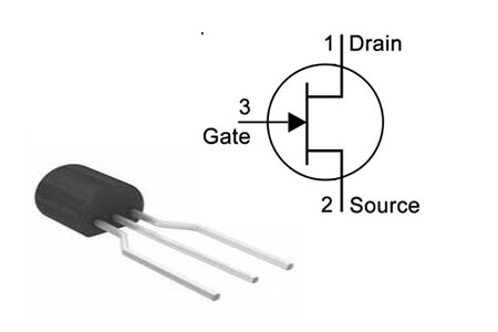
J113 Pinout

J113 Pinout

J113 CAD Model

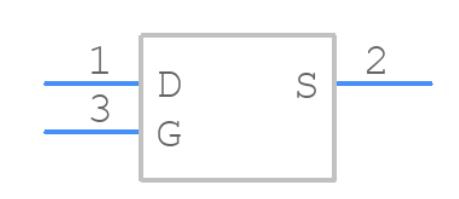
J113 Symbol


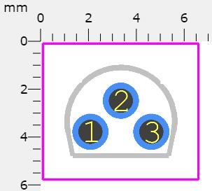
J113 Footprint


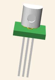
J113 3D Model

Specifications

ON Semiconductor J113_D75Z technical specifications, attributes, parameters and parts with similar specifications to ON Semiconductor J113_D75Z.

J113_D75Z Tech Specifications

ON Semiconductor J113_D75Z technical specifications, attributes, parameters and parts with similar specifications to ON Semiconductor J113_D75Z.

Product Attribute Attribute Value
Mounting TypeThrough Hole
Package / CaseTO-226-3, TO-92-3 (TO-226AA) (Formed Leads)
Supplier Device PackageTO-92-3
Operating Temperature-55°C~150°C TJ
PackagingTape & Box (TB)
Product Attribute Attribute Value
Part StatusObsolete
Moisture Sensitivity Level (MSL)1 (Unlimited)
Base Part NumberJ113
Power - Max625mW
FET TypeN-Channel
Product Attribute Attribute Value
Current - Drain (Idss) @ Vds (Vgs=0)2mA @ 15V
Voltage - Cutoff (VGS off) @ Id500mV @ 1μA
Voltage - Breakdown (V(BR)GSS)35V
Resistance - RDS(On)100Ohms
0 Products View Similar

J113 Features

  • Package-Type: TO-92  , SOT-23

  • Transistor Type: N Channel  JFET (Symmetrical)

  • Maximum Drain to Gate Voltage: 35V

  • Maximum Reverse Gate to Source Voltage: –35V

  • Maximum Continues Gate Current: 50mA

  • Maximum Gate to Source Cutoff Voltage:  –5 to –3V

  • Maximum Power Dissipation: 625mW

  • Max Storage & Operating temperature  should be: -55 to +150 °C

  • Drain and source  are exchangeable

Benefits of J113

  • High switching speed

  • Better response to the frequency 

  • Good accuracy

  • Low cost 

  • Low insertion loss etc.

J113 Applications

  • Audio preamplifiers

  • High gain amplifiers 

  • Sensor & detector circuits 

  • Current limiting circuits

  • Analog switching circuits

  • Low-level signal amplification 

Where and How to use J113?

J113 is suitable for a wide range of applications, including current limiting, chopper, and a variety of analog switching circuits. Aside from that, it can be used to boost the strength of any form of electronic signal in high gain amplifier applications.

Equivalents for J113

Part No. Manufacturer/Description
J111 RF   FET Transistor, 35 V, 625 mW, TO-92
   
ON SEMI
J112 ON SEMI
   
JFET Transistor, -35 V, 5 mA, -5 V, TO-92, JFET
   
 Each

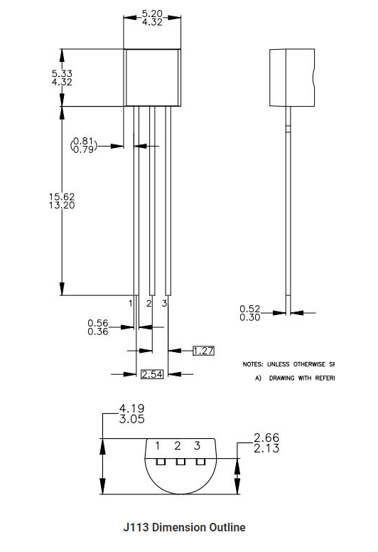
J113 Dimension Outline

J113 Dimension Outline

J113 Manufacturer

onsemi (formerly ON Semiconductor until August 5, 2021) is an American semiconductor supplier company, formerly in the Fortune 500, but dropping into the Fortune 1000 (ranked 512) in 2020.[3][1] Products include power and signal management, logic, discrete, and custom devices for automotive, communications, computing, consumer, industrial, LED lighting, medical, military/aerospace and power applications.

Frequently Asked Questions

What is J113 used for?
The J113 is a through-hole, N-channel switch in the TO-92 package. This device is designed for low-level analog switching, sample and holds circuits, and chopper stabilized amplifiers.
What is the voltage of j113?
Its supply voltage DC max is 30V.
What is the operating temperature of J113?
-55°C~150°C TJ
How does a JFET work?
A JFET is a three-terminal semiconductor device that uses one type of carriers, such as electrons or holes, to conduct current. The device's current conduction is controlled by an electric field that exists between the gate and the conducting channel. The JFET has a low noise level and a high input impedance.
FAQ
What is J113 used for?
The J113 is a through-hole, N-channel switch in the TO-92 package. This device is designed for low-level analog switching, sample and holds circuits, and chopper stabilized amplifiers.
What is the voltage of j113?
Its supply voltage DC max is 30V.
What is the operating temperature of J113?
-55°C~150°C TJ
How does a JFET work?
A JFET is a three-terminal semiconductor device that uses one type of carriers, such as electrons or holes, to conduct current. The device's current conduction is controlled by an electric field that exists between the gate and the conducting channel. The JFET has a low noise level and a high input impedance.

TAGS

Share