ATTENTION: Due to increased demand and order volume, processing time may take an additional 1-3 business days.
HomeCommunitySubjectKA7500B Controller: Features, Pinout, and Datasheet

KA7500B Controller: Features, Pinout, and Datasheet

IC REG CTRLR BUCK 16DIP Hello guys. The KA7500B is used for the control circuit of the PWM switching regulator. This article mainly introduces features, pinout, datasheet and other detailed information about ON Semiconductor KA7500B.

8898

Sep 27, 2021

Maxine Watt

1

How to test TL494 / KA7500 PWM Controller IC


IC REG CTRLR BUCK 16DIP

Hello guys. The KA7500B is used for the control circuit of the PWM switching regulator. This article mainly introduces features, pinout, datasheet and other detailed information about ON Semiconductor KA7500B.

KA7500B

1500In Stock
Min.: 1 Mult.: 1
Quantity Unit Price Ext. Price
1+ $0.85707$0.86
10+ $0.80855$8.09
100+ $0.76279$76.28
500+ $0.71961$359.81
1000+ $0.67888$678.88
Unit Price:$0.85707
Subtotal: $0.86
Looking for a better price? Want a lower wholesale price? Please send an RFQ, and we will respond immediately.
Quick Links

KA7500B Description

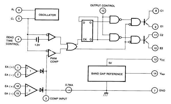
The KA7500B is used for the control circuit of the PWM switching regulator. The KA7500B consists of a 5V reference voltage circuit, two error amplifiers, a flip flop, an output control circuit, a PWM comparator, a dead time comparator and an oscillator. This device can be operated in the switching frequency of 1kHz to 300kHz.


KA7500B Pinout

Pinout


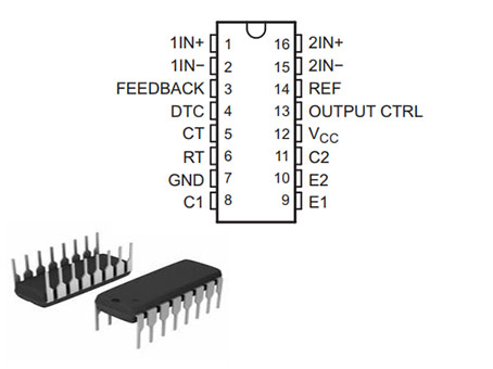
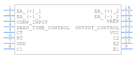
Pin Number Pin Name Description
1 1IN+ The non-inverting input terminal of error amplifier 1. In the closed-loop system, the given signal of the controlled quantity will be input to the error amplifier through this pin, while in the open-loop system, the pin needs to be grounded or left floating.
2 1IN- The inverting input terminal of the error amplifier 1. In the closed-loop system, the feedback signal of the controlled quantity will be input into the error amplifier through this pin. At this time, it is also necessary to connect the feedback network between this pin and pin 3. In the open-loop system, this pin is grounded or left floating.
3 FEEDBACK Feedback/PWM comparator input terminal. In a closed-loop system, different types of feedback networks can be connected between this pin and pin 2 as required to form various types of regulators such as proportional, proportional-integral, and integral to meet different user needs.
4 DTC The dead time controls the output of the comparator. This terminal is used to set the value of TL494 dead time. When this pin is grounded, the dead time is the smallest, and the maximum station-to-empty ratio can be obtained.
5 CT Oscillator timing capacitor access terminal. The value range of CT is usually between 0.001 and 0.1yF.
6 RT Oscillator timing resistor access terminal. The value range of the foot is usually between 5 to 100kQ.
7 GND Signal ground (reference ground for chip work).
8 C1 The collector terminal of the output transistor VT1, which is the positive pulse output terminal. In push-pull working mode, this terminal outputs a positive pulse signal, and pin 11 outputs a negative pulse signal. The phase difference between the two is 1800. After isolation and amplification, the switching tube is driven separately. In single-ended working mode, this terminal can be connected in parallel with pin 11 to improve the output capability of the pulse width modulation controller TL494.
9 E1 The emitter terminal of the output transistor VT1, this terminal is the reference ground terminal of the pin 8 output pulse signal and is generally directly connected to pin 7.
10 E2 The emitter terminal of the output transistor VT2, this terminal is the reference ground terminal of the pin 11 output pulse signal and is generally directly connected to pin 7.
11 C2 The collector terminal of the output transistor VT2, which is the reverse pulse output terminal. In the push-pull working mode, this terminal outputs a reverse pulse signal, and pin 8 outputs a forward pulse signal. The phase difference between the two is 1800. After isolation and amplification, they drive the switch tubes respectively. In single-ended working mode, this terminal can be connected in parallel with pin 8 to improve the output capability of the pulse width modulation controller TL494.
12 Vcc Bias power (chip working power) access terminal. In application, a filter capacitor with a capacity of 0.1UF or more must be connected to the common ground terminal.
13 OUTPUT CTRL Output working mode control terminal. Push-pull or single-ended output mode can be selected through this pin. When the terminal is connected to a high level, TL494 will work in push-pull mode, and the maximum duty cycle can reach 48% at this time. When the terminal is connected to a low level, the two output pulses are exactly the same, and the maximum duty cycle can reach 96%.
14 REF The input current of the reference power supply output can reach 10mA.
15 2IN- The inverted input terminal of the error amplifier 2. This terminal can be connected to the feedback signal of the protection circuit to realize fault protection such as over-current and over-voltage.
16 2IN+ The non-inverting input terminal of error amplifier 2. This terminal is the protection threshold voltage (current) setting terminal, which is used to realize fault protection such as overcurrent and overvoltage.

KA7500B CAD Model

Symbol

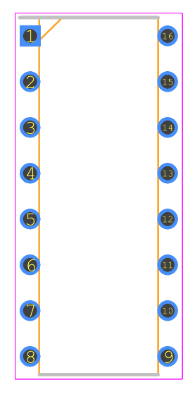
Footprint

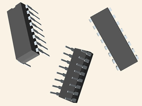
3D Model

KA7500B Features

• Internal Regulator Provides a Stable 5V Reference Supply Trimmed to 5%

• Uncommitted Output TR for 200mA Sink or Source Current

• Output Control For Push-Pull or Single Ended Operation

• Variable Duty Cycle By Dead Time Control Complete PWM Control Circuit

• On-Chip Oscillator With Master or Slave Operation

• Internal Circuit Prohibits Double Pulse at Either Output

Specifications

ON Semiconductor KA7500B technical specifications, attributes, parameters and parts with similar specifications to ON Semiconductor KA7500B.

KA7500B Tech Specifications

ON Semiconductor KA7500B technical specifications, attributes, parameters and parts with similar specifications to ON Semiconductor KA7500B.

Product Attribute Attribute Value
Lifecycle StatusACTIVE, NOT REC (Last Updated: 2 days ago)
Factory Lead Time19 Weeks
MountThrough Hole
Mounting TypeThrough Hole
Package / Case16-DIP (0.300, 7.62mm)
Number of Pins16Pins
Weight1.627826g
Operating Temperature0°C~70°C TA
PackagingTube
Published2002
JESD-609 Codee3
Pbfree Codeyes
Part StatusNot For New Designs
Moisture Sensitivity Level (MSL)1 (Unlimited)
Number of Terminations16Terminations
Product Attribute Attribute Value
ECCN CodeEAR99
Terminal FinishTin (Sn)
Terminal PositionDUAL
Terminal Pitch2.54mm
Base Part NumberKA7500
FunctionStep-Down
Number of Outputs1Output
Output TypeTransistor Driver
Operating Supply Voltage42V
Input Voltage-Nom20V
Analog IC - Other TypeSWITCHING CONTROLLER
Output ConfigurationPositive
Output Current250mA
Voltage - Supply (Vcc/Vdd)7V~42V
Control FeaturesDead Time Control
Product Attribute Attribute Value
Input Voltage (Min)7V
TopologyBuck
Control ModeVOLTAGE-MODE
Frequency - Switching1kHz~300kHz
Input Voltage (Max)40V
Control TechniquePULSE WIDTH MODULATION
Synchronous RectifierYes
Switcher ConfigurationSINGLE
Max Frequency300kHz
Duty Cycle (Max)45%
Clock SyncNo
Height Seated (Max)5.08mm
Width7.62mm
RoHS StatusROHS3 Compliant
0 Products View Similar

KA7500B Internal Block Diagram

Internal Block Diagram

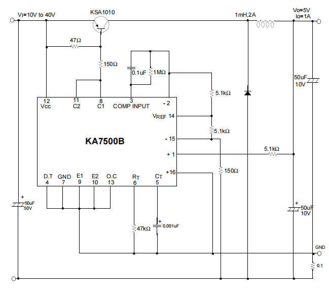
KA7500B Typical Application

Typical Application

KA7500B Alternatives

Part Number Description Manufacturer
LM78S40CJPOWER CIRCUITS 1.5A SWITCHING REGULATOR, 100kHz SWITCHING FREQ-MAX, CDIP16, CERAMIC, DIP-16 Texas Instruments
CS5150HGDR16POWER CIRCUITS Switching Controller, Voltage-mode, 1.5A, PDSO16, 0.150 INCH, SO-16 Cherry Semiconductor Corporation
SG2526JPOWER CIRCUITS Switching Controller, Voltage-mode, 0.2A, 350kHz Switching Freq-Max, BIPolar, CDIP16, HERMETIC SEALED, CERAMIC, DIP-16 Microsemi Corporation
SG1526JPOWER CIRCUITS Switching Controller, Voltage-mode, 0.2A, 400kHz Switching Freq-Max, CDIP18, CERAMIC, DIP-18 Motorola Semiconductor Products
CS-5151D16POWER CIRCUITS Switching Controller, Voltage-mode, 1.5A, 1000kHz Switching Freq-Max, BIPolar, PDSO16, Cherry Semiconductor Corporation
TL494CNPOWER CIRCUITS 0.5A SWITCHING CONTROLLER, 200kHz SWITCHING FREQ-MAX, PDIP16, 648-08 Motorola Mobility LLC
UPC494C-APOWER CIRCUITS Switching Controller, 0.25A, 300kHz Switching Freq-Max, BIPolar, PDIP16, 0.300 INCH, PLASTIC, DIP-16 NEC Electronics America Inc
CS5157GD16POWER CIRCUITS CPU 5-Bit Synchronous Buck Controller, SOIC 16 LEAD, 48-TUBE onsemi
5962-8876101EAPOWER CIRCUITS IC 1.5 A SWITCHING REGULATOR, CDIP16, CERAMIC, DIP-16, Switching Regulator or Controller Defense Supply Center Columbus
L6910GPOWER CIRCUITS Adjustable step down controller with synchronous rectification STMicroelectronics

KA7500B Applications

 5V Reference Source

• Sawtooth Oscillator

• Operational Amplifier

• Comparators

• Pulse Trigger

• Quiet Time Comparator


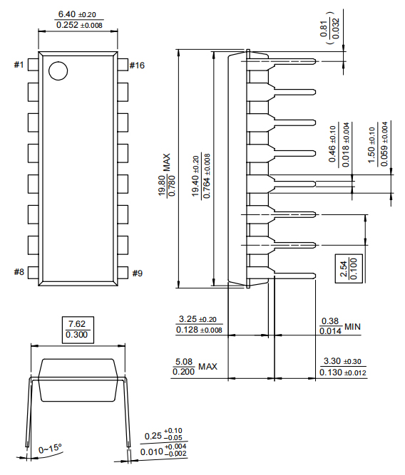
KA7500B Package

KA7500B Manufacturer

ON Semiconductor is a manufacturer dedicated to reducing energy use. It has a comprehensive combination of power, signal management and logic, energy-saving customized solutions. As a world-class high-reliability supply chain, it has a network of manufacturing facilities, sales, offices and design centers in major markets in North America, Europe and the Asia-Pacific region.

Datasheet PDF

Download datasheets and manufacturer documentation for ON Semiconductor KA7500B.

KA7500B Documents

Download datasheets and manufacturer documentation for KA7500B

Frequently Asked Questions

1.Is it normal that the input voltage of the KA7500B chip is only 6 volts?
The pin definition and function of KA7500B are the same as TL494, PWM controller, mostly used for switching power supply of half-bridge structure. To determine whether it is normal, first explain which pin is being tested. If it is a power supply pin, 6v cannot start the chip.
2.What model is used to replace the KA7500B manifold?
The same as TL494.
3.Can the original EST7502B of computer switching power supply control be replaced with KA7500B?
There may be a problem with the main control chip of the switching power supply. This chip is rarely used in the power supply. It is not clear whether it can be replaced with the KA7500B, but it is obvious that your power supply is malfunctioning.
FAQ
1.Is it normal that the input voltage of the KA7500B chip is only 6 volts?
The pin definition and function of KA7500B are the same as TL494, PWM controller, mostly used for switching power supply of half-bridge structure. To determine whether it is normal, first explain which pin is being tested. If it is a power supply pin, 6v cannot start the chip.
2.What model is used to replace the KA7500B manifold?
The same as TL494.
3.Can the original EST7502B of computer switching power supply control be replaced with KA7500B?
There may be a problem with the main control chip of the switching power supply. This chip is rarely used in the power supply. It is not clear whether it can be replaced with the KA7500B, but it is obvious that your power supply is malfunctioning.

TAGS

Share