ATTENTION: Due to increased demand and order volume, processing time may take an additional 1-3 business days.
HomeCommunitySubjectLF353N Dual JFET Input Op-Amp: Datasheet, Pinout and Equivalents

LF353N Dual JFET Input Op-Amp: Datasheet, Pinout and Equivalents

IC OPAMP JFET 2 CIRCUIT 8DIP LF353N is a wide bandwidth dual JFET operational amplifier. This article mainly covers datasheet, pinout, applications, equivalents, and other details about LF353N.

2248

Sep 6, 2021

Esther Ferguson

How to set up a circuit with an op amp (LF353)


IC OPAMP JFET 2 CIRCUIT 8DIP

LF353N is a wide bandwidth dual JFET operational amplifier. This article mainly covers datasheet, pinout, applications, equivalents, and other details about LF353N. Furthermore, there is a huge range of semiconductors, capacitors, resistors, and Ics in stock. Welcome RFQ!
LF353N

72000In Stock
Min.: 1 Mult.: 1
Price not displayed? Not available to buy online? Please send an RFQ, and we will respond immediately.
Quick Links

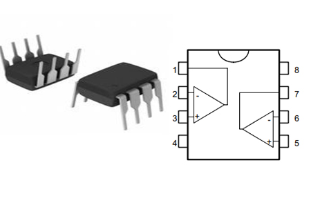
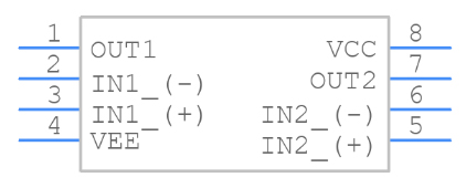
LF353N Pinout

Pin   Number Pin Name Description
1 OUTPUT-A The output of Op-Amp 1
2 INPUT- A(-) Inverting Input of   Op-Amp 1
3 INPUT- B(+) Non-Inverting Input   of Op-Amp 1
4 VEE, GND Ground or Negative   Supply Voltage
5 INPUT- B(+) Non-Inverting Input   of Op-Amp 2
6 INPUT- B(-) Inverting Input of   Op-Amp 2
7 OUTPUT B The output of Op-Amp 2
8 VCC Positive Supply   Voltage

LF353N CAD Model

Symbol

Symbol

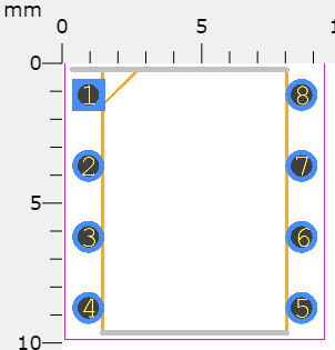
Footprint

Footprint


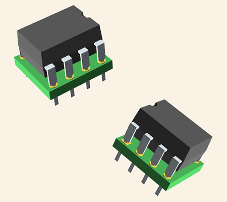
3D Model

3D Model

LF353N Description

These circuits are high-speed JFET input dual operational amplifiers incorporating well matched, high voltage JFET and bipolar transistors in a monolithic integrated circuit.

LF353N features high slew rates, low input bias and offset currents, and a low offset voltage temperature coefficient.


Specifications

ON Semiconductor LF353N technical specifications, attributes, parameters and parts with similar specifications to ON Semiconductor LF353N.

LF353N Tech Specifications

ON Semiconductor LF353N technical specifications, attributes, parameters and parts with similar specifications to ON Semiconductor LF353N.

Product Attribute Attribute Value
Factory Lead Time6 Weeks
MountThrough Hole
Mounting TypeThrough Hole
Package / Case8-DIP (0.300, 7.62mm)
Number of Pins8Pins
Weight851mg
Operating Temperature0°C~70°C
PackagingTube
JESD-609 Codee3
Pbfree Codeno
Part StatusLast Time Buy
Moisture Sensitivity Level (MSL)1 (Unlimited)
Number of Terminations8Terminations
ECCN CodeEAR99
Terminal FinishTin (Sn)
Terminal PositionDUAL
Number of Functions2Functions
Supply Voltage15V
Product Attribute Attribute Value
Base Part NumberLF353
Pin Count8
Operating Supply Voltage36V
Number of Channels2Channels
Max Supply Voltage18V
Operating Supply Current3.6mA
Nominal Supply Current6.5mA
Power Dissipation500mW
Max Supply Current6.5mA
Slew Rate13V/μs
ArchitectureVOLTAGE-FEEDBACK
Amplifier TypeJ-FET
Common Mode Rejection Ratio70 dB
Current - Input Bias50pA
Input Offset Voltage (Vos)10mV
Bandwidth4MHz
Neg Supply Voltage-Nom (Vsup)-15V
Unity Gain BW-Nom4000 kHz
Product Attribute Attribute Value
Voltage Gain100dB
Power Supply Rejection Ratio (PSRR)70dB
Low-OffsetNO
Frequency CompensationYES
Voltage - Input Offset5mV
Max Dual Supply Voltage18V
Low-BiasYES
Min Dual Supply Voltage5V
Dual Supply Voltage9V
Input Offset Current-Max (IIO)0.004μA
Height3.3mm
Length9.27mm
Width6.35mm
REACH SVHCNo SVHC
Radiation HardeningNo
RoHS StatusROHS3 Compliant
Lead FreeLead Free
0 Products View Similar

LF353N Schematic Diagram

LF353N Features

  • Low power consumption

  • Wide common-mode (up to VCC+) and differential voltage range

  • Low input bias and offset current

  • Output short-circuit protection

  • High input impedance JFET input stage

  • Internal frequency compensation

  • Latch-up free operation

  • High slew rate 16 V/µs (typical)

LF353N Applications

  • Low-noise Audio circuits

  • High-Input Impedance designs

  • Sample and Hold Circuit

  • High-Speed Integrator

LF353N Application Circuit

LF353N Alternatives

Manufacturers Category Description
Fairchild Operational   Amplifiers(General Purpose) FAIRCHILD   SEMICONDUCTOR LF353N Operational Amplifier, Dual, 2 Amplifier, 4MHz, 13V/µs,   ± 18V, DIP, 8Pins
TI Operational   Amplifiers(General Purpose) Operational   Amplifier, Dual, 2 Amplifier, 4MHz, 13V/µs, ± 15V, DIP, 8Pins
ADI Operational   Amplifiers(General Purpose) ANALOG devises AD712KNZ Operational Amplifier, Dual, 2 Amplifier, 4MHz, 20V/µs, ± 4.5V to ±   18V, DIP, 8Pins
TI Operational   Amplifiers(General Purpose) TEXAS INSTRUMENTS   LF412CN/NOPB Operational Amplifier, Dual, 2 Amplifier, 4MHz, 15V/µs, 10V to   36V, DIP, 8Pins

LF353N vs. LF353P

The LF353N is a Dual Operational Amplifier with an internally compensated input offset voltage. The LF353P is a high-speed JFET-input Operational Amplifier with very low input offset voltage. It requires a low supply current yet maintains a large gain-bandwidth product and a fast slew rate.

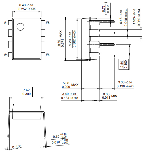
LF353N Package

LF353N Manufacturer

ON Semiconductor is a semiconductor supplier company, formerly in the Fortune 500, but dropping into the Fortune 1000 (ranked 512) in 2020. Products include power and signal management, logic, discrete, and custom devices for automotive, communications, computing, consumer, industrial, LED lighting, medical, military/aerospace, and power applications. ON Semiconductor runs a network of manufacturing facilities, sales offices, and design centers in North America, Europe, and the Asia Pacific regions. Headquartered in Phoenix, Arizona, ON Semiconductor has revenues of $3.907 billion (2016), which puts it among the worldwide top 20 semiconductor sales leaders.

Datasheet PDF

LF353N Documents

Download datasheets and manufacturer documentation for LF353N

PCN Obsolescence/ EOL
Mult Dev EOL 4/Nov/2019
PCN Design/Specification
MDIP 05/Oct/2016
Logo 17/Aug/2017
Environmental Information
Material Declaration LF353N

Frequently Asked Questions

What can be LF353N used for?
The LF353N can be used in applications such as high-speed integrators, digital-to-analog converters, sample-and-hold circuits, and many other circuits. The LF353 is characterized for operation from 0°C to 70°C.
What is the difference between LF353N and LF353P?
The LF353N is a Dual Operational Amplifier with an internally compensated input offset voltage. The LF353P is a high-speed JFET-input Operational Amplifier with very low input offset voltage. It requires a low supply current yet maintains a large gain-bandwidth product and a fast slew rate.
What is the difference between LF353N and LF356?
The performance of these two OPs is very close, and both belong to the CMOS input OP. Relatively speaking, the LF356 has a low slew rate (not good for large signals), a slightly larger bandwidth, and a slightly smaller offset current. If it is only for ordinary use, it can be substituted. Pay attention to dual op-amp and single op-amp.
FAQ
What can be LF353N used for?
The LF353N can be used in applications such as high-speed integrators, digital-to-analog converters, sample-and-hold circuits, and many other circuits. The LF353 is characterized for operation from 0°C to 70°C.
What is the difference between LF353N and LF353P?
The LF353N is a Dual Operational Amplifier with an internally compensated input offset voltage. The LF353P is a high-speed JFET-input Operational Amplifier with very low input offset voltage. It requires a low supply current yet maintains a large gain-bandwidth product and a fast slew rate.
What is the difference between LF353N and LF356?
The performance of these two OPs is very close, and both belong to the CMOS input OP. Relatively speaking, the LF356 has a low slew rate (not good for large signals), a slightly larger bandwidth, and a slightly smaller offset current. If it is only for ordinary use, it can be substituted. Pay attention to dual op-amp and single op-amp.

TAGS

Share