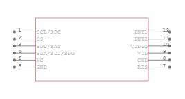
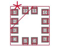
The Vdd line provides power to the device core, while the Vdd IO line provides power to the I/O pads. Decoupling capacitors for the power supply (100 nF ceramic, 10 fF aluminium) should be put as close to pin 9 of the device as practicable (common design practice).
To ensure optimal IC behaviour, all voltage and ground supplies must be present at the same time (see the LIS2DW12TR electrical connections (top view) diagram below). Without stopping the communication bus, it is feasible to delete Vdd while keeping Vdd IO; in this case, the measurement chain is turned off.
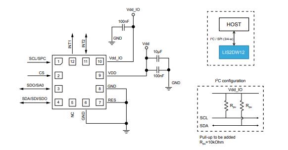
LIS2DW12 electrical connections (top view)
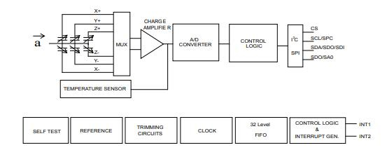
The device's functionality as well as the measured acceleration data can be selected and accessed via the I2C or SPI interfaces. CS must be tied high (i.e. attached to Vdd IO) while utilizing I2C.
The user can entirely configure the functions, threshold, and timing of the two interrupt pins (INT1 and INT2) using the I2C/SPI interface.