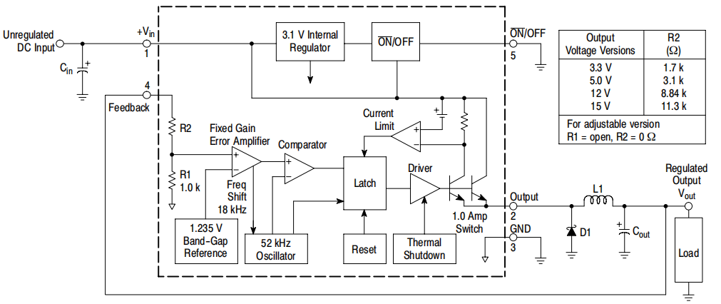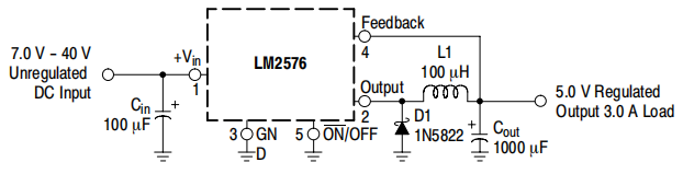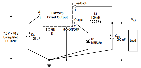
Fixed Output Voltage Versions
Cin − 100 μF, 75 V, Aluminium Electrolytic
Cout − 1000 μF, 25 V, Aluminium Electrolytic
D1 − Schottky, MBR360
L1 − 100 μH, Pulse Eng. PE−92108
R1 − 2.0 k, 0.1%
R2 − 6.12 k, 0.1%
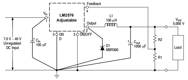
Adjustable Output Voltage Versions
Vout=Vref*( 1.0+R2/R1)
R2=R1*(Vout/Vref-1.0)
Where Vref = 1.23 V, R1
between 1.0 k and 5.0 k
The layout of the printed circuit board is critical in any switching regulator. Voltage transients caused by rapidly switching currents caused by wiring inductance, stray capacitance, and parasitic inductance of printed circuit board traces can cause electromagnetic interference (EMI) and disrupt the desired operation. To minimize inductance and ground loops, the length of the leads indicated by thick lines should be kept as short as possible, as shown in the typical test circuit above.
Single point grounding (as stated) or ground plane construction should be used for the greatest results.
In order to avoid coupling to sensitive electronics, the PCB area linked to the LM2576's Pin 2 (emitter of the internal switch) should be reduced to a minimum.
The feedback is another delicate component of the circuit. It's critical to keep the sensitive feedback wiring as short as possible. When utilizing the adjustable version of the LM2576 regulator, physically put the programming resistors near the regulator to ensure this.