ATTENTION: Due to increased demand and order volume, processing time may take an additional 1-3 business days.
HomeCommunitySubjectLM53601LQDSXTQ1: Pinout, Automotive, Step-Down, Converter

LM53601LQDSXTQ1: Pinout, Automotive, Step-Down, Converter

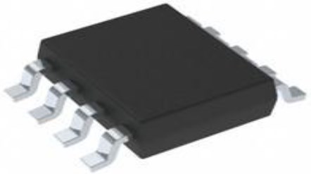
PMIC - Voltage Regulators - DC DC Switching Regulators SWITCHING REGULATOR 10-WFDFN Exposed Pad -40°C~150°C TJ 2.1MHz 0.5mm LM53601 Automotive, AEC-Q100 IC REG BUCK 5V 1A SYNC 10WSON

137

Dec 15, 2021

Hogan Edward

PMIC - Voltage Regulators - DC DC Switching Regulators SWITCHING REGULATOR 10-WFDFN Exposed Pad -40°C~150°C TJ 2.1MHz 0.5mm LM53601 Automotive, AEC-Q100 IC REG BUCK 5V 1A SYNC 10WSON

The synchronous buck regulator LM53601LQDSXTQ1 is built for automotive applications, with output voltages of 5 V, 3.3 V, or an adjustable output. The following article will introduce the features, pinout, datasheet, etc, of the device.

LM53601LQDSXTQ1

50In Stock
Min.: 1 Mult.: 1
Quantity Unit Price Ext. Price
1+ $7.56552$7.57
10+ $7.13728$71.37
100+ $6.73329$673.33
500+ $6.35216$3176.08
1000+ $5.9926$5992.6
Unit Price:$7.56552
Subtotal: $7.57
Looking for a better price? Want a lower wholesale price? Please send an RFQ, and we will respond immediately.
Quick Links

LM53601LQDSXTQ1 Description

The synchronous buck regulator LM53601LQDSXTQ1 is built for automotive applications, with output voltages of 5 V, 3.3 V, or an adjustable output. TheLM53601LQDSXTQ1 can handle up to 1000 mA. The device boasts advanced high-speed circuitry that allows it to regulate from an input of 18 V to a 3.3 V output at a fixed frequency of 2.1 MHz. The device's innovative architecture allows it to regulate a 3.3-V output from a 3.8-V input voltage. Input surge protection can be designed with a voltage range of up to 36 V and a transient tolerance of up to 42 V.

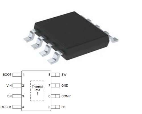
LM53601LQDSXTQ1 Pinout

LM53601LQDSXTQ1 CAD Model

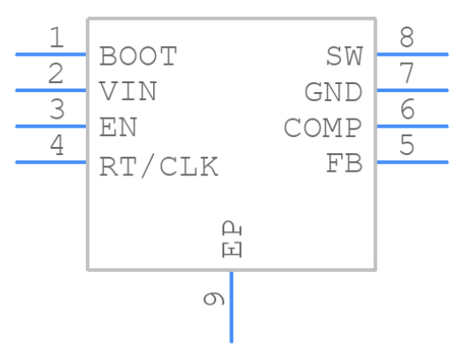
Symbol


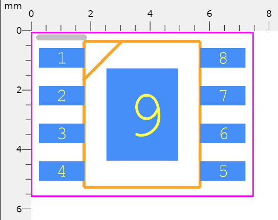
Footprint


3D Model

LM53601LQDSXTQ1 Features

•  Qualified for automotive applications

•  AEC-Q100 qualified with the following results:

– Device temperature grade 1: –40°C to 125°C ambient operating temperature range

– Device HBM classification level 2

– Device CDM classification level C5

•  –40°C to 150°C junction temperature range(available)

•  Wide operating input voltage: 3.55 V to 36 V (with transient to 42 V)

•  Spread spectrum option available

•  2.1-MHz fixed switching frequency

•  Low quiescent current: 23 μA

•  Shutdown current: 1.8 μA

•  Adjustable, 3.3-V, or 5-V output

•  Maximum current load: 650 mA for LM53600-Q1,1000 mA for LM53601-Q1

•  Pin-selectable forced PWM mode

•  RESET output with filter and delay release

•  External frequency synchronization

•  Internal compensation, soft start, current limit, and UVLO

•  10-lead, 3-mm × 3-mm SON package with wettable and non-wettable flanks


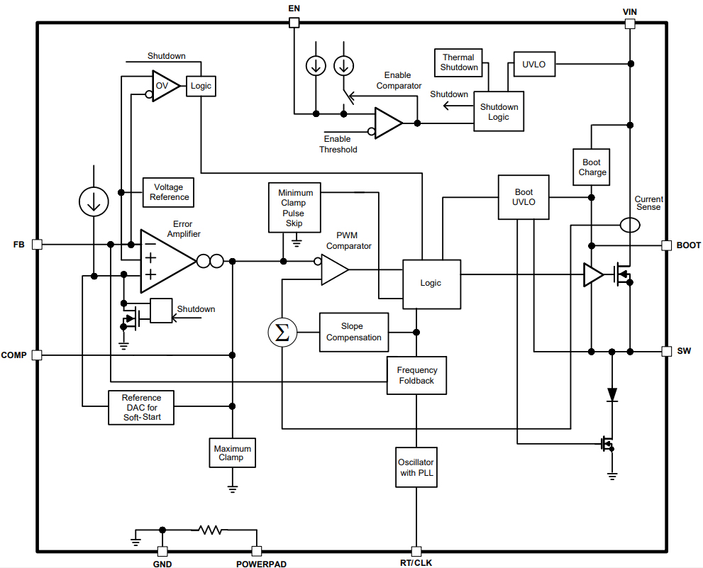
LM53601LQDSXTQ1 Functional Block Diagram

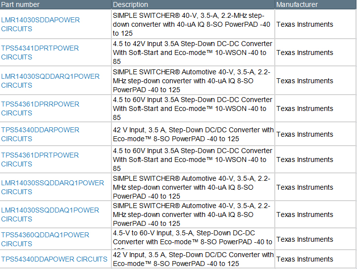
LM53601LQDSXTQ1 Equivalents

Specifications

NA LM53601LQDSXTQ1 technical specifications, attributes, parameters and parts with similar specifications to NA LM53601LQDSXTQ1.

LM53601LQDSXTQ1 Tech Specifications

Texas Instruments LM53601LQDSXTQ1 technical specifications, attributes, parameters and parts with similar specifications to Texas Instruments LM53601LQDSXTQ1.

Product Attribute Attribute Value
Lifecycle StatusACTIVE (Last Updated: 1 day ago)
Factory Lead Time6 Weeks
MountSurface Mount
Mounting TypeSurface Mount
Package / Case10-WFDFN Exposed Pad
Number of Pins10Pins
Usage LevelAutomotive grade
Operating Temperature-40°C~150°C TJ
PackagingTape & Reel (TR)
SeriesAutomotive, AEC-Q100
JESD-609 Codee3
Pbfree Codeyes
Part StatusActive
Moisture Sensitivity Level (MSL)2 (1 Year)
Number of Terminations10Terminations
Product Attribute Attribute Value
ECCN CodeEAR99
Terminal FinishMatte Tin (Sn)
Additional FeatureALSO OPERATES IN PFM CONTROL TECHNIQUE
Terminal PositionDUAL
Terminal FormNO LEAD
Terminal Pitch0.5mm
Base Part NumberLM53601
FunctionStep-Down
Number of Outputs1Output
Voltage - Input (Max)36V
Output Voltage5V
Output TypeFixed
Voltage - Input (Min)3.8V
Input Voltage-Nom13.5V
Analog IC - Other TypeSWITCHING REGULATOR
Product Attribute Attribute Value
Output ConfigurationPositive
Quiescent Current23μA
TopologyBuck
Control ModeCURRENT-MODE
Frequency - Switching2.1MHz
Control TechniquePULSE WIDTH MODULATION
Synchronous RectifierYes
Min Output Voltage5V
Height800μm
Length3mm
Width3mm
Thickness750μm
RoHS StatusROHS3 Compliant
Lead FreeLead Free
0 Products View Similar

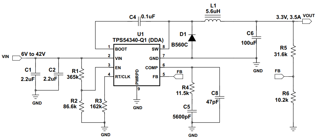
LM53601LQDSXTQ1 Typical Application Circuit

LM53601LQDSXTQ1 Typical Application Circuit

LM53601LQDSXTQ1 Manufacturer

Texas Instruments Incorporated (TI) is an American technology company based in Dallas, Texas, that designs and manufactures semiconductors and various integrated circuits, which it sells to electronics designers and manufacturers globally. It is one of the top 10 semiconductor companies worldwide based on sales volume. The company's focus is on developing analog chips and embedded processors, which account for more than 80% of its revenue. TI also produces TI digital light processing technology and education technology products including calculators, microcontrollers, and multi-core processors. The company boasts 45,000 patents around the globe as of 2016.

Frequently Asked Questions

What is LM53601LQDSXTQ1?
The synchronous buck regulator LM53601LQDSXTQ1 is built for automotive applications, with output voltages of 5 V, 3.3 V, or an adjustable output. TheLM53601LQDSXTQ1 can handle up to 1000 mA. The device boasts advanced high-speed circuitry that allows it to regulate from an input of 18 V to a 3.3 V output at a fixed frequency of 2.1 MHz. The device's innovative architecture allows it to regulate a 3.3-V output from a 3.8-V input voltage. Input surge protection can be designed with a voltage range of up to 36 V and a transient tolerance of up to 42 V.
What is the recommended operative temperature of the device?
-40℃-150℃.
FAQ
What is LM53601LQDSXTQ1?
The synchronous buck regulator LM53601LQDSXTQ1 is built for automotive applications, with output voltages of 5 V, 3.3 V, or an adjustable output. TheLM53601LQDSXTQ1 can handle up to 1000 mA. The device boasts advanced high-speed circuitry that allows it to regulate from an input of 18 V to a 3.3 V output at a fixed frequency of 2.1 MHz. The device's innovative architecture allows it to regulate a 3.3-V output from a 3.8-V input voltage. Input surge protection can be designed with a voltage range of up to 36 V and a transient tolerance of up to 42 V.
What is the recommended operative temperature of the device?
-40℃-150℃.

TAGS

Share