ATTENTION: Due to increased demand and order volume, processing time may take an additional 1-3 business days.
HomeCommunitySubjectLP5569RTWR 9 CHANNEL RGB DRIVER

LP5569RTWR 9 CHANNEL RGB DRIVER

Texas Instruments LP5569RTWR I2C RGB LED Driver is a programmable, easy-to-use 9-channel I2C LED driver designed to produce lighting effects for various applications.

56

Mar 8, 2022

Tyrone Evans

Texas Instruments LP5569RTWR I2C RGB LED Driver is a programmable, easy-to-use 9-channel I2C LED driver designed to produce lighting effects for various applications. This passage is going to introduce LP5569RTWR from the perspectives of the datasheet, pinout, and other ways.


LP5569RTWR

12000In Stock
Min.: 1 Mult.: 1
Quantity Unit Price Ext. Price
1+ $2.13282$2.13
10+ $2.0121$20.12
100+ $1.8982$189.82
500+ $1.79076$895.38
1000+ $1.68939$1689.39
Unit Price:$2.13282
Subtotal: $2.13
Looking for a better price? Want a lower wholesale price? Please send an RFQ, and we will respond immediately.
Quick Links

LP5569RTWR Description

The LP5569RTWR  is a programmable, easy-to-use 9  -channel I2C  LED driver that may be used to create various lighting effects. The LED driver includes an internal SRAM memory for user-programmed sequences as well as three programmable LED engines for operation without the usage of a processor. When the processor is put into sleep mode, autonomous functioning minimizes system power usage.

Even with a 2.5  -V input voltage, a high-efficiency charge pump can drive LEDs with high VF. By autonomously selecting the appropriate charge-pump gain depending on LED forward voltage needs, the LP5569RTWR   LED driver maintains good efficiency throughout a wide operating voltage range. When LEDs are not active, the LP5569RTWR  gadget enters power-saving mode, significantly reducing idle-current usage.


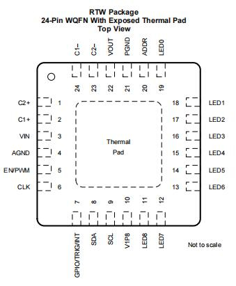
LP5569RTWR Pins and Pins Functions


PIN TYPE DESCRIPTION
NAME NO.
ADDR 20 I I2C slave-address selection pin.
AGND 4 G Analog and digital ground. Connect to PGND, exposed thermal pad, and common ground plane.
C1- 24 A Negative pin of charge-pump flying capacitor 1. If a charge pump is not used, this pin must be left floating.
C1+ 2 A Positive pin of charge-pump flying capacitor 1. If a charge pump is not used, this pin must
be left floating.
C2- 23 A Negative pin of charge-pump flying capacitor 2. If a charge pump is not used, this pin must
be left floating.
C2+ 1 A Positive pin of charge-pump flying capacitor 2. If a charge pump is not used, this pin must
be left floating.
CLK 6 I, OD Clock input/output. By default, this pin is a clock input. If not used, this pin must be
connected to GND or VIN.
EN/PWM 5 I Chip enable and PWM input pin.
GPIO/TRIG/INT 7 I, OD General-purpose input or open-drain output, trigger input or open-drain output, or interrupt open-drain output. This pin function is configured in the I2C registers. By default, this pin is a general-purpose output (open-drain) and can be left floating if not used.
LED0 19 A LED current sink 0. If not used, this pin can be left floating.
LED1 18 A LED current sink 1. If not used, this pin can be left floating.
LED2 17 A LED current sink 2. If not used, this pin can be left floating.
LED3 16 A LED current sink 3. If not used, this pin can be left floating.
LED4 15 A LED current sink 4. If not used, this pin can be left floating.
LED5 14 A LED current sink 5. If not used, this pin can be left floating.
LED6 13 A LED current sink 6. If not used, this pin can be left floating.
LED7 12 A LED current sink 7. If not used, this pin can be left floating.
LED8 11 A LED current sink 8. If not used, this pin can be left floating.
PGND 21 G Charge-pump power ground. Connect to AGND, exposed thermal pad, and common
ground plane.
SCL 9 I I2C bus clock line. If not used, this pin must be connected to GND or VIN.
SDA 8 I, OD I2C bus data line. If not used, this pin must be connected to GND or VIN.
V1P8 10 P Input power for digital circuitry.
VIN 3 P Input power, a 1-µF capacitor must be connected between PGND and this pin.
VOUT 22 A Charge-pump output voltage. If a charge pump is used, a 1-µF capacitor must be
connected between PGND and this pin. If charge pump is not used or is used in 1×
the mode only, the capacitor can be omitted.

LP5569RTWR Feature

  • Supply Voltage Range: 2.5 V–5.5 V • Nine High-Accuracy Current Sinks

– 25.5 mA Maximum per Channel 

– 8-Bit Individual Current Control

– 12-Bit 20-kHz Internal Individual PWM Control Without Audio Noise

  • Three Programmable LED Engines

– Independent Illumination Control Without Active Microcontroller Control

– Synchronization Among Multiple Devices 

– Up to 256 Instructions in SRAM Memory  for Storing Sequences of Lighting Patterns 

– LP5523  - and LP5523  1-Device-Compatible Command Set

  • Flexible Dimming Control

– I2C Dimming Control

– PWM Direct-Input Dimming 

– PWM Input Frequency: 100-Hz to 20-kHz

  • Adaptive High-Efficiency Charge-Pump Control for driving High  -VF LEDs  With Low Battery Voltage

  • Master Fader Control Allows Dimming of MultipleLEDs by Writing to Only One Register to Reduce the I2C Bus Traffic

  • 2-µA Low Standby Current  and 10-µA in automatic Power-Save Mode When LEDs  AreInactive

  • POR, UVLO, and TSD Protections 

LP5569RTWR CAD Models

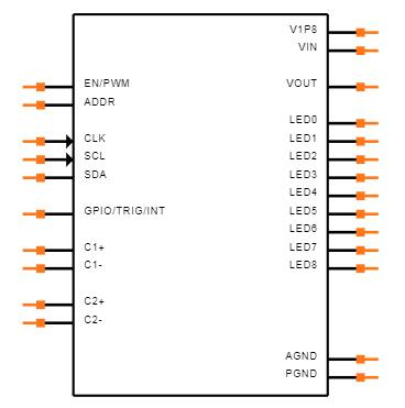
Symbol

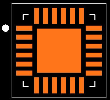
Footprint

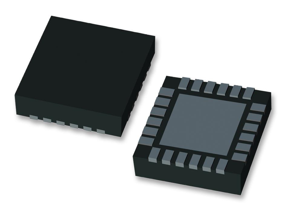
3D Models

Specifications

LP5569RTWR Tech Specifications

Texas Instruments LP5569RTWR technical specifications, attributes, parameters and parts with similar specifications to Texas Instruments LP5569RTWR.

Product Attribute Attribute Value
Lifecycle StatusACTIVE (Last Updated: 2 days ago)
Factory Lead Time6 Weeks
Mounting TypeSurface Mount
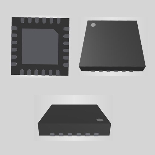
Package / Case24-WFQFN Exposed Pad
Surface MountYES
Number of Pins24Pins
SwitchingFrequency1.25MHz
Operating Temperature-40°C~85°C
PackagingTape & Reel (TR)
JESD-609 Codee4
Pbfree Codeyes
Part StatusActive
Moisture Sensitivity Level (MSL)2 (1 Year)
Number of Terminations24Terminations
Product Attribute Attribute Value
TypeLinear
Terminal FinishNickel/Palladium/Gold (Ni/Pd/Au)
ApplicationsGeneral Purpose
Terminal PositionQUAD
Number of Functions1Function
Supply Voltage3.6V
Terminal Pitch0.5mm
Base Part NumberLP5569
Number of Outputs9Outputs
Output Voltage5.5V
Max Supply Voltage5.5V
Min Supply Voltage2.5V
Output Current160mA
TopologySwitched Capacitor (Charge Pump)
Product Attribute Attribute Value
Internal Switch(s)No
fmax-Min0.4 MHz
DimmingI2C, PWM
Number of Segments9Segments
Max Junction Temperature (Tj)125°C
Voltage - Supply (Min)2.5V
Multiplexed Display CapabilityNO
Ambient Temperature Range High85°C
Data Input ModeSERIAL
Height800μm
Length4mm
Width4mm
Thickness750μm
RoHS StatusROHS3 Compliant
0 Products View Similar

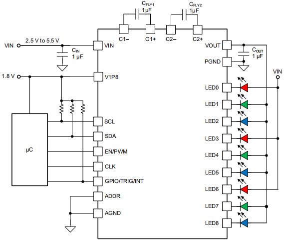
LP5569RTWR Applications Circuit

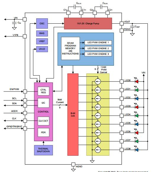
LP5569RTWR Functional Block Diagram

LP5569RTWR Manufacturer

Texas Instruments Incorporated (TI) is an American technology company based in Dallas, Texas, that designs and manufactures semiconductors and integrated circuits for electronic designers and manufacturers around the world. Based on sales volume, it is one of the top ten semiconductor companies in the world. Analog chips and embedded processors, which account for more than 80  % of the company's revenue, are the company's main focus. TI also makes calculators, microcontrollers, and multi-core processors, as well as TI digital light processing technology and education technology,  As of 2016, the company had 45,000  patents worldwide.

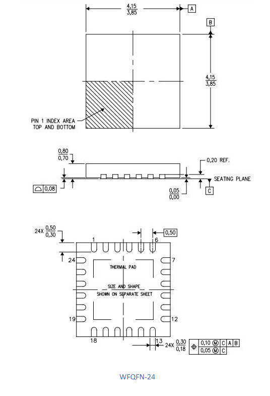
LP5569RTWR Package

LP5569RTWR Advantages

  1. Current Sinks

The LP5569RTWR   LED drivers are constant-current sources. Maximum output-current scale can be programmed by control registers up to 25.5 mA.

  1. Charge Pump

The LP5569RTWR  device includes a pre-regulated switched-capacitor charge pump with a programmable voltage multiplication of 1× or 1.5×.

  1. Energy Efficiency

The red LED  (R) element of an RGB LED  typically has a forward voltage of about 2 V. these LED s can be powered directly from the input voltage because battery voltage is typically high enough to drive red LED  s over the whole operating voltage range.

  1. Automatic Power-Save Mode

When the LED  outputs are not active, the LP5569RTWR  device is able to enter power-save mode automatically, thus lowering idle-current consumption down to TBD μA (typical). Automatic power-save mode is enabled when the MISC register (address 2Fh) POWERSAVE_EN bit = 1.

  1. Protection Features

It has four protection features, including Thermal Shutdown, Undervoltage Lockout  (UVLO), Power-On Reset  (POR), LED  Fault Detection

  1. Clock Generation and Synchronization 

The LP5569RTWR  device can generate a 32-kHz clock signal and use it for synchronizing multiple devices. The CLK pin is configured as an input by default 

P5569RTWR Dimensions

Height 800μm
Length 4mm
Thickness 750μm
Width 4mm

Datasheet PDF

LP5569RTWR Documents

Download datasheets and manufacturer documentation for LP5569RTWR

Frequently Asked Questions

What is LP5569RTWR?
The LP5569RTWR device is a fully integrated lighting management unit for producing lighting effects for various LED applications. The LP5569RTWR device includes all necessary power management, low-side current sinks, a two-wire serial I2C-compatible interface, and programmable LED engines.
Does LP5569RTWR have protection features?
Yes, its protection features include power-on reset, charge-pump, input-current limiter, thermal shutdown(TSD), and under-voltage lockout(UVLO).
Can LP5569RTWR be operated in 100℃?
No, its operating temperature is between -40 and 85℃.
Where is LP5569RTWR made from?
It is made by an American company-Texas Instruments Incorporated.
What’s the main parameters of LP5569RTWR?
the main parameters of this part are: Nine-channel I2C RGB LED driver with engine control and charge pump 24-WQFN -40 to 85.
FAQ
What is LP5569RTWR?
The LP5569RTWR device is a fully integrated lighting management unit for producing lighting effects for various LED applications. The LP5569RTWR device includes all necessary power management, low-side current sinks, a two-wire serial I2C-compatible interface, and programmable LED engines.
Does LP5569RTWR have protection features?
Yes, its protection features include power-on reset, charge-pump, input-current limiter, thermal shutdown(TSD), and under-voltage lockout(UVLO).
Can LP5569RTWR be operated in 100℃?
No, its operating temperature is between -40 and 85℃.
Where is LP5569RTWR made from?
It is made by an American company-Texas Instruments Incorporated.
What’s the main parameters of LP5569RTWR?
the main parameters of this part are: Nine-channel I2C RGB LED driver with engine control and charge pump 24-WQFN -40 to 85.

TAGS

Share