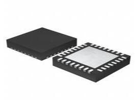
IC MCU 32BIT 32KB FLASH 32HVQFN
This article will unlock more detailed information about LPC824M201JHI33E, a 32-bit ARM® Cortex®-M0 microcontroller.

IC MCU 32BIT 32KB FLASH 32HVQFN This article will unlock more detailed information about LPC824M201JHI33E, a 32-bit ARM? Cortex?-M0+ microcontroller.
116
Aug 19, 2021
Darlene Bunyan
IC MCU 32BIT 32KB FLASH 32HVQFN
This article will unlock more detailed information about LPC824M201JHI33E, a 32-bit ARM® Cortex®-M0 microcontroller.
LPC824M201JHI33E
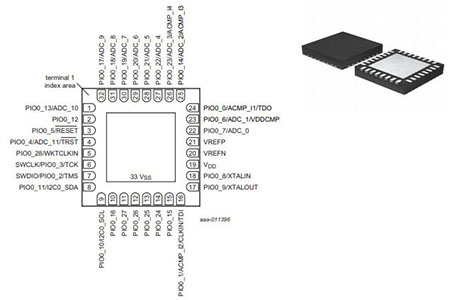
Symbol
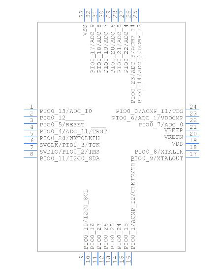
Footprint
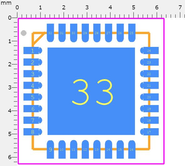
3D Model
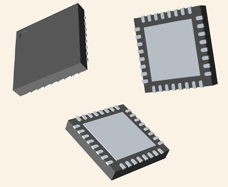
LPC824M201JHI33E is a 32-bit ARM® Cortex®-M0+ microcontroller from the LPC82x family operating at CPU frequencies of up to 30 MHz. And the LPC82x support up to 32 KB of flash memory and 8 KB of SRAM.
NXP USA Inc. LPC824M201JHI33E technical specifications, attributes, parameters and parts with similar specifications to NXP USA Inc. LPC824M201JHI33E.
NXP USA Inc. LPC824M201JHI33E technical specifications, attributes, parameters and parts with similar specifications to NXP USA Inc. LPC824M201JHI33E.
| Product Attribute | Attribute Value | |
|---|---|---|
| Factory Lead Time | 12 Weeks | |
| Mounting Type | Surface Mount | |
| Package / Case | 32-VFQFN Exposed Pad | |
| Surface Mount | YES | |
| Number of Pins | 32Pins | |
| Data Converters | A/D 12x12b | |
| Number of I/Os | 29I/Os | |
| ROM(word) | 32768 | |
| Operating Temperature | -40°C~105°C TA | |
| Packaging | Tray | |
| Series | LPC82x | |
| Published | 2005 | |
| Part Status | Discontinued | |
| Moisture Sensitivity Level (MSL) | 3 (168 Hours) | |
| Number of Terminations | 33Terminations | |
| Additional Feature | SEATED HGT-NOM |
| Product Attribute | Attribute Value | |
|---|---|---|
| Voltage - Supply | 3.3V | |
| Terminal Position | QUAD | |
| Terminal Form | NO LEAD | |
| Peak Reflow Temperature (Cel) | 260 | |
| Terminal Pitch | 0.5mm | |
| Time@Peak Reflow Temperature-Max (s) | NOT SPECIFIED | |
| Base Part Number | LPC824M201 | |
| JESD-30 Code | S-PQCC-N33 | |
| Oscillator Type | Internal | |
| Speed | 30MHz | |
| RAM Size | 8K x 8 | |
| uPs/uCs/Peripheral ICs Type | MICROCONTROLLER, RISC | |
| Core Processor | ARM® Cortex®-M0+ | |
| Peripherals | Brown-out Detect/Reset, DMA, POR, PWM, WDT | |
| Clock Frequency | 25MHz | |
| Program Memory Type | FLASH |
| Product Attribute | Attribute Value | |
|---|---|---|
| Core Size | 32-Bit | |
| Program Memory Size | 32KB 32K x 8 | |
| Connectivity | I2C, SPI, UART/USART | |
| Bit Size | 32 | |
| Has ADC | YES | |
| DMA Channels | YES | |
| PWM Channels | YES | |
| DAC Channels | NO | |
| On Chip Program ROM Width | 8 | |
| Voltage - Supply (Max) | 3.6V | |
| Voltage - Supply (Min) | 1.8V | |
| Length | 5mm | |
| Height Seated (Max) | 0.85mm | |
| Width | 5mm | |
| RoHS Status | ROHS3 Compliant |
lSystem:
ARM Cortex-M0+ processor (revision r0p1), running at frequencies of up to 30 MHz with single-cycle multiplier and fast single-cycle I/O port.
ARM Cortex-M0+ built-in Nested Vectored Interrupt Controller (NVIC).
System tick timer.
AHB multilayer matrix.
Serial Wire Debug (SWD) with four breakpoints and two watchpoints. JTAG boundary-scan (BSDL) supported.
MTB
lMemory:
Up to 32 KB on-chip flash programming memory with 64 Byte page write and erase. Code Read Protection (CRP) supported.
8 KB SRAM.
lROM API support:
Boot loader.
On-chip ROM APIs for ADC, SPI, I2C, USART, power configuration (power profiles) and integer divide.
Flash In-Application Programming (IAP) and In-System Programming (ISP).
lDigital peripherals:
High-speed GPIO interface connected to the ARM Cortex-M0+ IO bus with up to 29 General-Purpose I/O (GPIO) pins with configurable pull-up/pull-down resistors, programmable open-drain mode, input inverter, and digital filter. GPIO direction control supports independent set/clear/toggle of individual bits.
High-current source output driver (20 mA) on four pins.
High-current sink driver (20 mA) on two true open-drain pins.
GPIO interrupt generation capability with boolean pattern-matching feature on eight GPIO inputs.
Switch matrix for flexible configuration of each I/O pin function.
CRC engine.
DMA with 18 channels and 9 trigger inputs.
lTimers:
State Configurable Timer (SCTimer/PWM) with input and output functions (including capture and match) for timing and PWM applications. Each SCTimer/PWM input is multiplexed to allow selecting from several input sources such as pins, ADC interrupt, or comparator output.
Four-channel Multi-Rate Timer (MRT) for repetitive interrupt generation at up to four programmable, fixed rates.
Self-Wake-up Timer (WKT) clocked from either the IRC, a low-power, low-frequency internal oscillator, or an external clock input in the always-on power domain.
Windowed Watchdog timer (WWDT).
l Analog peripherals:
One 12-bit ADC with up to 12 input channels with multiple internal and external trigger inputs and with sample rates of up to 1.2 Msamples/s. The ADC supports two independent conversion sequences.
Comparator with four input pins and external or internal reference voltage.
l Serial peripherals:
Three USART interfaces with pin functions assigned through the switch matrix and one common fractional baud rate generator.
Two SPI controllers with pin functions are assigned through the switch matrix.
Four I2C-bus interfaces. One I2C supports Fast-mode Plus with 1 Mbit/s data rates on two true open-drain pins and listen mode. Three I2Cs support data rates up to 400 kbit/s on standard digital pins.
l Clock generation:
12 MHz internal RC oscillator trimmed to 1.5 % accuracy that can optionally be used as a system clock.
Crystal oscillator with an operating range of 1 MHz to 25 MHz.
Programmable watchdog oscillator with a frequency range of 9.4 kHz to 2.3 MHz.
PLL allows CPU operation up to the maximum CPU rate without the need for a high-frequency crystal. May be run from the system oscillator, the external clock input, or the internal RC oscillator.
Clock output function with divider that can reflect all internal clock sources.
l Power control:
Power consumption in active mode as low as 90 uA/MHz in low-current mode using the IRC as the clock source.
Integrated PMU (Power Management Unit) to minimize power consumption.
Reduced power modes: Sleep mode, Deep-sleep mode, Power-down mode, and Deep power-down mode.
Wake-up from Deep-sleep and Power-down modes on activity on USART, SPI, and
I2C peripherals.
Timer-controlled self wake-up from Deep power-down mode
Power-On Reset (POR).
Brownout detects (BOD).
lUnique device serial number for identification.
lSingle power supply (1.8 V to 3.6 V).
lOperating temperature range is -40 °C to +105 °C.
l Available in a TSSOP20 and HVQFN33 (5x5) package.
Sensor gateways
Simple motor control
Industrial
Portables and wearables
Gaming controllers
Lighting
8/16-bit applications
Motor control
Consumer
Fire and security applications
Climate control
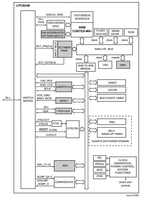
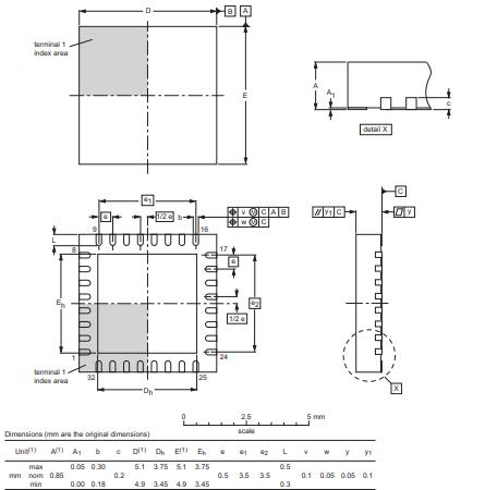
NXP Semiconductors provides mixed signal and standard products based on its security, identification, automotive, networking, radio frequency, analogue signal, and power management expertise.
Download datasheets and manufacturer documentation for NXP USA Inc. LPC824M201JHI33E.
Download datasheets and manufacturer documentation for LPC824M201JHI33E
TAGS
Comments