ATTENTION: Due to increased demand and order volume, processing time may take an additional 1-3 business days.
HomeCommunitySubjectMicrocontroller PIC18F2550, PIC18F2550 Pins, PIC18F2550 Datasheet and Programming [Video]

Microcontroller PIC18F2550, PIC18F2550 Pins, PIC18F2550 Datasheet and Programming [Video]

Embedded - Microcontrollers A/D 10x10b 28-DIP (0.300, 7.62mm) 32kB Brown-out Detect/Reset, HLVD, POR, PWM, WDT -40°C~85°C TA 4.2V~5.5V PIC? 18F MICROCONTROLLER PIC18F2550 48MHz IC MCU 8BIT 32KB FLASH 28SDIP

72

Nov 10, 2021

Nigel Frances

How to program PIC18F | Blinking an LED step by step


Embedded - Microcontrollers A/D 10x10b 28-DIP (0.300, 7.62mm) 32kB Brown-out Detect/Reset, HLVD, POR, PWM, WDT -40°C~85°C TA 4.2V~5.5V PIC® 18F MICROCONTROLLER PIC18F2550 48MHz IC MCU 8BIT 32KB FLASH 28SDIP

PIC18F2550 is a High-Performance, Enhanced flash, USB Microcontroller with NANO-Watt-Technology. This article is going to explain pins, datasheet pdf, programming, features, and other details about the PIC18F2550 USB microcontroller.

PIC18F2550-I/SP

4280In Stock
Min.: 1 Mult.: 1
Quantity Unit Price Ext. Price
1+ $16.85743$16.86
10+ $15.90324$159.03
100+ $15.00305$1500.31
500+ $14.15382$7076.91
1000+ $13.35266$13352.66
Unit Price:$16.85743
Subtotal: $16.86
Looking for a better price? Want a lower wholesale price? Please send an RFQ, and we will respond immediately.
Quick Links

What is PIC18F2550?

PIC18F2550 is a High-Performance, Enhanced flashUSB Microcontroller with NANO-Watt-Technology. PIC18F2550 microcontroller is an 8-bit microcontroller designed by MICROCHIP. It is one of the cheapest microcontrollers of the PIC18FXXXX  series. It is popular due to its performance, cheapness, and multiple features.

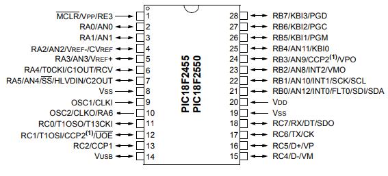
PIC18F2550 Pinout

Because a controller has so many features, the manufacturer cannot offer  I/O  pins for all of them. Many of the controller's pins have numerous functions. By default, these functionalities are turned off; however, they can be turned on through programming. Each pin's function will be briefly described below.

 PIC18F2550 Pinout


Pin   Number Pin Name Description
1 MCLR/VPP/RE3 MCLR: Master   Clear(RESET) Input VPP: programming voltage input RE3: I/O pin of PORTE, PIN 3
2 RA0/AN0 RA0: I/O pin of   PORTA, PIN 0 AN0: Analog input 0
3 RA1/AN1 RA1: I/O pin of   PORTA, PIN 1 AN1: Analog input 1
4 RA2/AN2/VREF-/CVREF RA2: I/O pin of   PORTA, PIN 2 AN2: Analog input 2 VREF-: A/D reference voltage (low) input   CVREF: Analog comparator reference output
5 RA3/AN3/VREF+ RA3: I/O pin of   PORTA, PIN 3 AN3: Analog input3 VREF+: A/D reference voltage (high) input
6 RA4/T0CKI/C1OUT/RCV RA4: I/O pin of   PORTA, PIN 4 T0CKI: Timer0 external clock input C1OUT: Comparator 1 output   RCV: External USB transceiver RCV input
7 RA5/AN4/SS/HLVDIN/C2OUT RA5: I/O pin of   PORTA, PIN 5 AN4: Analog input 4 SS: SPI slave select input HLDVIN:   High/Low-Voltage Detect input C2OUT: Comparator 2 output
8 VSS Ground
9 OSC1/CLKI OSC1:Oscillator pin 1   CLKI: External clock source input
10 OSC2/CLKO/RA6 OSC2: Oscillator pin   2 CLKO: clock source output RA6: I/O pin of PORTA, PIN 6
11 RC0/T1OSO/T13CKI RC0: I/O pin of   PORTC, PIN 0 T1OSO: Timer1 oscillator output T13CKI: Timer1/Timer3 external   clock input
12 RC1/T1OSI/CCP2/UOE RC1: I/O pin of   PORTC, PIN 1 T1OSI: Timer1 oscillator input CCP2:Capture 2 input/Compare 2   output/PWM2 output UOE: External USB transceiver OE output
13 RC2/CCP1 RC2: I/O pin of   PORTC, PIN 2 CCP1: Capture 1 input/Compare 1 output/PWM1 output.
14 VUSB VUSB: Internal USB   3.3V voltage regulator output
15 RC4/D-/VM RC4: I/O pin of   PORTC, PIN 4 D-: USB differential minus line (input/output) VM: External USB   transceiver VM input
16 RC5/D+/VP RC5: I/O pin of   PORTC, PIN 5 D+: USB differential plus line (input/output). VP: External USB   transceiver VP input
17 RC6/TX/CK RC6: I/O pin of   PORTC, PIN 6 TX: EUSART asynchronous transmit CK: EUSART synchronous clock   (see RX/DT).
18 RC7/RX/DT/SDO RC7: I/O pin of   PORTC, PIN 7 RX: EUSART asynchronous receive DT: EUSART synchronous data (see   TX/CK). SDO: SPI data out
19 VSS Ground
20 VDD Positive Power Supply   (+5V)
21 RB0/AN12/INT0/FLT0/SDI/SDA RB0: I/O pin of   PORTB, PIN 0 AN12: Analog input 12 INT0: External interrupt 0 FLT0: Enhanced   PWM Fault input (ECCP1 module) SDI: SPI data in SDA: I2C data I/O
22 RB1/AN10/INT1/SCK/SCL RB1: I/O pin of   PORTB, PIN 1 AN10: Analog input 10 INT1: External interrupt 1 SCK:   Synchronous serial clock input/output for SPI mode SCL: Synchronous serial   clock input/output for I2C mode
23 RB2/AN8/INT2/VMO RB2: I/O pin of   PORTB, PIN 2 AN8: Analog input 8 INT2: External interrupt 2 VMO: External USB   transceiver VMO output
24 RB3/AN9/CCP2/VPO RB3: I/O pin of   PORTB, PIN 3 AN9: Analog input 9 CCP2: Capture 2 input/Compare 2 output/PWM2   output VPO: External USB transceiver VPO output
25 RB4/AN11/KBI0 RB4: I/O pin of   PORTB, PIN 4 AN11: Analog input 11 KBI0: Interrupt-on-change pin
26 RB5/KBI1/PGM RB5: I/O pin of   PORTB, PIN 5 KBI1: Interrupt-on-change pin PGM: Low-Voltage ICSP Programming   enable pin
27 RB6/KBI2/PGC RB6: I/O pin of   PORTB, PIN 6 KBI2: Interrupt-on-change pin PGC: In-Circuit Debugger and ICSP   programming clock pin.
28 RB7/KBI3/PGD RB7: I/O pin of   PORTB, PIN 7 KBI3: Interrupt-on-change pin PGD: In-Circuit Debugger and ICSP   programming data pin.

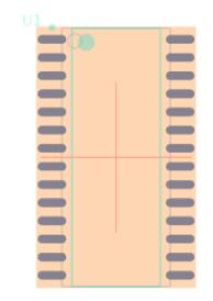
PIC18F2550 CAD Model

PIC18F2550 Symbol

PIC18F2550 Footprint

Specifications

Microchip Technology PIC18F2550-I/SP technical specifications, attributes, parameters and parts with similar specifications to Microchip Technology PIC18F2550-I/SP.

PIC18F2550-I/SP Tech Specifications

Microchip Technology PIC18F2550-I/SP technical specifications, attributes, parameters and parts with similar specifications to Microchip Technology PIC18F2550-I/SP.

Product Attribute Attribute Value
Factory Lead Time2 Weeks
MountThrough Hole
Mounting TypeThrough Hole
Package / Case28-DIP (0.300, 7.62mm)
Number of Pins28Pins
Weight9.071847g
Data ConvertersA/D 10x10b
Number of I/Os24I/Os
Watchdog TimersYes
Operating Temperature-40°C~85°C TA
PackagingTube
SeriesPIC® 18F
Published2004
JESD-609 Codee3
Pbfree Codeyes
Part StatusActive
Moisture Sensitivity Level (MSL)1 (Unlimited)
Number of Terminations28Terminations
Terminal FinishMatte Tin (Sn) - annealed
Max Power Dissipation1W
Product Attribute Attribute Value
Terminal PositionDUAL
Supply Voltage5V
Frequency48MHz
Base Part NumberPIC18F2550
Pin Count28
Supply Voltage-Max (Vsup)5.5V
InterfaceI2C, SPI, UART, USART, USB
Memory Size32kB
Oscillator TypeInternal
Nominal Supply Current1.1mA
RAM Size2K x 8
Voltage - Supply (Vcc/Vdd)4.2V~5.5V
uPs/uCs/Peripheral ICs TypeMICROCONTROLLER
Number of Bits8Bits
Core ProcessorPIC
PeripheralsBrown-out Detect/Reset, HLVD, POR, PWM, WDT
Program Memory TypeFLASH
Core Size8-Bit
Program Memory Size32KB 16K x 16
ConnectivityI2C, SPI, UART/USART, USB
Product Attribute Attribute Value
Bit Size8
Access Time48 μs
Has ADCYES
DMA ChannelsNO
Data Bus Width8b
Number of Timers/Counters4Timers/Counters
Address Bus Width8b
Density256 kb
EEPROM Size256 x 8
CPU FamilyPIC
Number of A/D Converters1A/D Converter
Number of ADC Channels10ADC Channels
Number of PWM Channels2PWM Channels
Height3.81mm
Length35.56mm
Width7.493mm
REACH SVHCNo SVHC
Radiation HardeningNo
RoHS StatusROHS3 Compliant
Lead FreeLead Free
0 Products View Similar

PIC18F2550 Features

CPU 8-bit
Total Number   of Pins 28
Operating   Voltage '+4.0 to +5.5 V   (+5.5V being absolute maximum)
Number of    programmable I/O pins 24
ADC Module 10channels, 10-bit   resolution ADC
Timer Module One8-bit counter,   Three16-bit counter
Analog   Comparators 2
PWM channels 2
External   Oscillator Up to 48MHz
Internal   Oscillator 32KHz-8MHz    Calibrated Internal Oscillator
Program memory   Type Flash
Program memory   / Flash memory 32Kbytes[10000   write/erase cycles]
CPU Speed 12 MIPS
RAM 2KBytes
EEPROM memory 256Bytes
Watchdog Timer Programmable Watchdog   Timer with Separate On-chip oscillator
Power Save   Modes Available
Operating   Temperature -40°C to +85°C(+85   being absolute maximum, -40 being the absolute minimum)

PIC18F2550 Replacements

PIC18F2455, PIC18F4455, PIC18F4550


PIC18F2550 Applications

  • It is used with those devices which required an interface with a PC.

  • Most of the smart application uses PIC18F2550 because it fills almost all the communication protocol of most of the applications.

How to Use PIC18F2550?

The PIC18F2550 is used in the same way as any other microcontroller,  Microcontrollers are not like digital ICs, which require only the connection of electricity to function. Before getting the chip to work, the microcontroller has to be programmed. To get the PIC18F2550 to work, we must first save the correct software file to the controller's FLASH memory. Once the controller receives power, it runs the code stored in FLASH memory to generate the answer.

PIC18F2550 Programming

  • List the functions to be executed by PIC18F2550

  • Write these functions in ‘IDE software’ using a supported programming  language

     (MPLAB  IDE  for Windows OS [www.microchip.com/mplabx-ide-windows-installer ] )

     (For these MPLAB  IDE you can use ‘C’ language to write the application program)

  • After writing the desired program compile for error elimination using IDE.

  • After successful compilation IDE application generates a HEX file for the written program.

  • Choose the programming device (usually ‘PIC kit 3’) which establishes communication between PC and PIC18F2550.

  • Run the HEX file dumping software which is related to the chosen programming device.

  • Choose the appropriate program HEX file.

  • Burn the HEX file (generated for the written program) in PIC18F2550 flash memory using this program.

  • Disconnect the programmer and connect the appropriate peripherals for the controller.

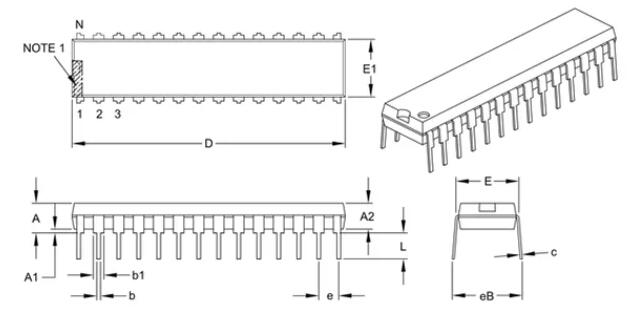
PIC18F2550 Package Dimensions

PIC18F2550 Package Dimensions

PIC18F2550 Manufacturer

Microchip Technology Inc. is a leading provider of microcontroller and analog semiconductors, providing low-risk product development, lower total system cost, and faster time to market for thousands of diverse customer applications worldwide. Headquartered in Chandler, Arizona, Microchip offers outstanding technical support along with dependable delivery and quality.

Datasheet PDF

Download datasheets and manufacturer documentation for Microchip Technology PIC18F2550-I/SP.

PIC18F2550-I/SP Documents

Download datasheets and manufacturer documentation for PIC18F2550-I/SP

Frequently Asked Questions

What is the use of PIC18F2550?
It is known as in-circuit serial programming, which uses a special programming circuit designed by the company to MICROCHIP to program the microcontroller using the HEX file of the program.
How many timers are available in PIC18 microcontroller?
A PIC18 microcontroller may have up to 5 timers: Timer0…Timer 4. - Timer0, Timer1, and Timer3 are 16-bit timers whereas Timer2 and Timer4 are 8-bit. - When a timer rolls over, an interrupt may be generated if it is enabled.
What is the voltage of PIC18F2550?
Its operating voltage is +4.0 to +5.5 V.
FAQ
What is the use of PIC18F2550?
It is known as in-circuit serial programming, which uses a special programming circuit designed by the company to MICROCHIP to program the microcontroller using the HEX file of the program.
How many timers are available in PIC18 microcontroller?
A PIC18 microcontroller may have up to 5 timers: Timer0…Timer 4. - Timer0, Timer1, and Timer3 are 16-bit timers whereas Timer2 and Timer4 are 8-bit. - When a timer rolls over, an interrupt may be generated if it is enabled.
What is the voltage of PIC18F2550?
Its operating voltage is +4.0 to +5.5 V.

TAGS

Share