ATTENTION: Due to increased demand and order volume, processing time may take an additional 1-3 business days.
HomeCommunitySubjectMJE13009 NPN Power Transistor: Datasheet, Pinout and Circuit

MJE13009 NPN Power Transistor: Datasheet, Pinout and Circuit

MJE13009 is a 12 AMPERE NPN silicon power transistor featuring 400 VOLTS ? 100 WATTS. This post mainly introduces the datasheet, power, circuit, equivalent, pinout, and more details about transistor MJE13009.

209

Sep 30, 2021

Bowen Saxton

MJE13009 check transistor MJE13009


TRANS NPN 400V 12A TO220AB

MJE13009 is a 12 AMPERE NPN silicon power transistor featuring 400 VOLTS − 100 WATTS. This post mainly introduces the datasheet, power, circuit, equivalent, pinout, and more details about transistor MJE13009. Furthermore, there is a huge range of semiconductors, capacitors, resistors, and ICs in stock. Welcome your RFQ!
MJE13009

18680In Stock
Min.: 1 Mult.: 1
Price not displayed? Not available to buy online? Please send an RFQ, and we will respond immediately.
Quick Links

MJE13009 Pinout

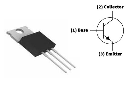
The pinout diagram for MJE13009 is shown in the diagram below.

Different doping concentrations are carried by the terminals. In comparison to other terminals, the collector pin is minimally doped, whereas the emitter pin is heavily doped. Similarly, the collector terminal is 10-times more doped than the base pin.

MJE13009 Pinout


Pin No Pin Name
1 Base
2 Collector
3 Emitter
4 Case (Collector)

MJE13009 CAD Model

MJE13009 Symbol


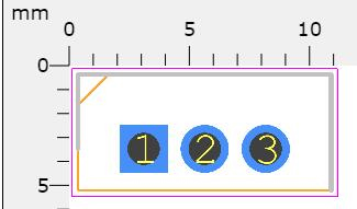
MJE13009 Footprint


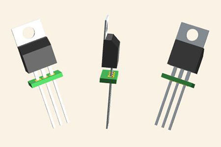
MJE13009 3D Model


MJE13009 Description

The MJE13009 is a high-voltage, high-speed power switching inductive circuit with a critical fall time. Switching Regulators, Inverters, Motor Controls, Solenoid/Relay Drivers, and Deflection Circuits are among the many 115 and 220 V switch-mode applications that they are well suited for.

Specifications

ON Semiconductor MJE13009 technical specifications, attributes, parameters and parts with similar specifications to ON Semiconductor MJE13009.

MJE13009 Tech Specifications

ON Semiconductor MJE13009 technical specifications, attributes, parameters and parts with similar specifications to ON Semiconductor MJE13009.

Product Attribute Attribute Value
Lifecycle StatusOBSOLETE (Last Updated: 1 week ago)
MountThrough Hole
Mounting TypeThrough Hole
Package / CaseTO-220-3
Number of Pins3Pins
Transistor Element MaterialSILICON
Collector-Emitter Breakdown Voltage400V
Collector-Emitter Saturation Voltage1V
Number of Elements1 Element
hFEMin8
Operating Temperature-65°C~150°C TJ
PackagingTube
Published2006
JESD-609 Codee0
Pbfree Codeno
Part StatusObsolete
Product Attribute Attribute Value
Moisture Sensitivity Level (MSL)1 (Unlimited)
Number of Terminations3Terminations
ECCN CodeEAR99
Terminal FinishTin/Lead (Sn/Pb)
Additional FeatureLEADFORM OPTIONS ARE AVAILABLE
Voltage - Rated DC400V
Max Power Dissipation2W
Peak Reflow Temperature (Cel)240
Reach Compliance Codenot_compliant
Current Rating12A
Time@Peak Reflow Temperature-Max (s)30
Pin Count3
Qualification StatusNot Qualified
Element ConfigurationSingle
Power Dissipation2W
Case ConnectionCOLLECTOR
Product Attribute Attribute Value
Transistor ApplicationSWITCHING
Gain Bandwidth Product4MHz
Polarity/Channel TypeNPN
Transistor TypeNPN
Collector Emitter Voltage (VCEO)3V
Max Collector Current12A
DC Current Gain (hFE) (Min) @ Ic, Vce8 @ 5A 5V
JEDEC-95 CodeTO-220AB
Vce Saturation (Max) @ Ib, Ic3V @ 3A, 12A
Transition Frequency4MHz
Collector Base Voltage (VCBO)700V
Emitter Base Voltage (VEBO)9V
RoHS StatusNon-RoHS Compliant
Lead FreeContains Lead
0 Products View Similar

MJE13009 Features

  • VCEO (sus) 400 V and 300 V

  • Reverse Bias SOA with Inductive Loads @ TC = 100C

  • Inductive Switching Matrix 3 to 12 Amp, 25 and 100C tc @ 8 A, 100C is 120 ns (Typ)

  • 700 V Blocking Capabilities

  • SOA and Switching Applications Information

  • Pb−Free Package is Available*


MJE13009 Alternatives

MJE1100, MJE1101, MJE1102, MJE1103, MJE1123, MJE12007


MJE13009 Applications

  • Switching Regulators

  • Inverters

  • Motor Controls

  • Solenoid/Relay drivers and Deflection circuits


MJE13009 Working Principle

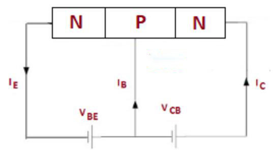
mje13009 circuit .jpg

MJE13009 Circuit

The total transistor operation is controlled by the base pin. When voltage is added to the base pin, the device is biased, and currently begins to flow from the collector to the emitter terminal.

The absence of symmetry within the transistor device is due to the varied doping concentrations of all these terminals.

Bipolar junction transistors are not symmetrical, which means that if you swap the collector and emitter terminals, the terminals will stop behaving in forward active mode and start acting in reverse mode. The value of both common-emitter and common-base current gains can be influenced by this terminal swapping.

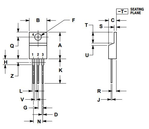
MJE13009 Dimension

 MJE13009 Dimension

MJE13009 Manufacturer

On Semiconductor (Nasdaq: ON) is a manufacturer engaging itself in reducing energy use. It features a comprehensive portfolio of power, signal management, and logic, custom solutions that are energy efficient. It acts as a world-class supply chain with high reliability and a network of manufacturing facilities, sales, offices, and design centers in key markets through North America, Europe, and the Asia Pacific regions.

Datasheet PDF

Download datasheets and manufacturer documentation for ON Semiconductor MJE13009.

MJE13009 Documents

Download datasheets and manufacturer documentation for MJE13009

Frequently Asked Questions

What us the use of MJE13009?
The MJE13009 is designed for high–voltage, high–speed power switching inductive circuits where fall time is critical. They are particularly suited for 115 and 220 V switch mode applications such as Switching Regulators, Inverters, Motor Controls, Solenoid/Relay drivers, and Deflection circuits.
When to use PNP vs. NPN?
Thus the most common use for NPN devices is for switching the ground side of a circuit. PNP devices are used to switch from the positive side. For example, consider the simple case of a load and a voltage source.
How does MJE13009 work?
MJE13009 is a type of bipolar junction transistor that belongs to the NPN transistor family where electrons are the major charge carriers. In NPN transistors current flows from the collector to emitter terminal while in the case of the PNP transistor current flows from emitter to collector terminal.
Can BLD137D be replaced with MJE13009?
BLD137D cannot be replaced with MJE13009. The withstand voltage of the two is no problem, but the collector power and dissipation power of the latter are much smaller than the former.
Can c3306 tube be replaced with MJE13009 if it is broken?
C3306 is 500v10A100w and MJE13009 is 700v12A100w. The latter parameter is greater than the former, so it can be replaced directly.
FAQ
What us the use of MJE13009?
The MJE13009 is designed for high–voltage, high–speed power switching inductive circuits where fall time is critical. They are particularly suited for 115 and 220 V switch mode applications such as Switching Regulators, Inverters, Motor Controls, Solenoid/Relay drivers, and Deflection circuits.
When to use PNP vs. NPN?
Thus the most common use for NPN devices is for switching the ground side of a circuit. PNP devices are used to switch from the positive side. For example, consider the simple case of a load and a voltage source.
How does MJE13009 work?
MJE13009 is a type of bipolar junction transistor that belongs to the NPN transistor family where electrons are the major charge carriers. In NPN transistors current flows from the collector to emitter terminal while in the case of the PNP transistor current flows from emitter to collector terminal.
Can BLD137D be replaced with MJE13009?
BLD137D cannot be replaced with MJE13009. The withstand voltage of the two is no problem, but the collector power and dissipation power of the latter are much smaller than the former.
Can c3306 tube be replaced with MJE13009 if it is broken?
C3306 is 500v10A100w and MJE13009 is 700v12A100w. The latter parameter is greater than the former, so it can be replaced directly.

TAGS

Share