ATTENTION: Due to increased demand and order volume, processing time may take an additional 1-3 business days.
HomeCommunitySubjectMTB30P06VT4G MOSFET: Pinout, Features and Datasheet [FAQ]

MTB30P06VT4G MOSFET: Pinout, Features and Datasheet [FAQ]

Trans MOSFET P-CH 60V 30A 3-Pin(2+Tab) D2PAK T/R The MTB30P06VT4G Power MOSFET is designed to withstand high energy in the avalanche and commutation modes.

286

Apr 29, 2022

Adair Toland

How Does a MOSFET Work?


Trans MOSFET P-CH 60V 30A 3-Pin(2 Tab) D2PAK T/R

The MTB30P06VT4G Power MOSFET is designed to withstand high energy in the avalanche and commutation modes. Furthermore, Huge range of Semiconductors, Capacitors, Resistors and IcS in stock. Welcome RFQ.


MTB30P06VT4G

5000In Stock
Min.: 1 Mult.: 1
Price not displayed? Not available to buy online? Please send an RFQ, and we will respond immediately.
Quick Links

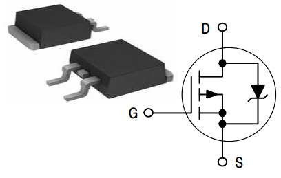
MTB30P06VT4G Pinout

The following figure is the diagram of MTB30P06VT4G Pinout.

Pinout

MTB30P06VT4G Description

The MTB30P06VT4G Power MOSFET is designed to withstand high energy in the avalanche and commutation modes. Designed for low voltage, high speed switching applications in power supplies, converters and power motor controls, these devices are particularly well suited for bridge circuits where diode speed and commutating safe operating areas are critical and offer additional safety margin against unexpected voltage transients.

This article provides you with a basic overview of the MTB30P06VT4G MOSFET, including its pin descriptions, features and specifications, etc., to help you quickly understand what MTB30P06VT4G is.

MTB30P06VT4G Features

• Avalanche Energy Specified

• IDSS and VDS(on) Specified at Elevated Temperature

• AEC−Q101 Qualified and PPAP Capable − MTBV30P06V

• These Devices are Pb−Free and are RoHS Compliant

Specifications

ON Semiconductor MTB30P06VT4G technical specifications, attributes, parameters and parts with similar specifications to ON Semiconductor MTB30P06VT4G.

MTB30P06VT4G Tech Specifications

ON Semiconductor MTB30P06VT4G technical specifications, attributes, parameters and parts with similar specifications to ON Semiconductor MTB30P06VT4G.

Product Attribute Attribute Value
Lifecycle StatusLAST SHIPMENTS (Last Updated: 3 days ago)
Mounting TypeSurface Mount
Package / CaseTO-263-3, D2Pak (2 Leads + Tab), TO-263AB
Surface MountYES
Number of Pins3Pins
Transistor Element MaterialSILICON
Current - Continuous Drain (Id) @ 25℃30A Tc
Drive Voltage (Max Rds On, Min Rds On)10V
Number of Elements1 Element
Power Dissipation (Max)3W Ta 125W Tc
Turn Off Delay Time98 ns
Operating Temperature-55°C~175°C TJ
PackagingTape & Reel (TR)
Published2006
JESD-609 Codee3
Pbfree Codeyes
Part StatusObsolete
Moisture Sensitivity Level (MSL)1 (Unlimited)
Number of Terminations2Terminations
Product Attribute Attribute Value
ECCN CodeEAR99
Resistance80MOhm
Terminal FinishTin (Sn)
Additional FeatureAVALANCHE RATED
Voltage - Rated DC-60V
Terminal FormGULL WING
Peak Reflow Temperature (Cel)260
Current Rating-30A
Time@Peak Reflow Temperature-Max (s)40
Pin Count3
JESD-30 CodeR-PSSO-G2
Element ConfigurationSingle
Operating ModeENHANCEMENT MODE
Power Dissipation3W
Case ConnectionDRAIN
Turn On Delay Time14.7 ns
FET TypeP-Channel
Transistor ApplicationSWITCHING
Rds On (Max) @ Id, Vgs80m Ω @ 15A, 10V
Product Attribute Attribute Value
Vgs(th) (Max) @ Id4V @ 250μA
Input Capacitance (Ciss) (Max) @ Vds2190pF @ 25V
Gate Charge (Qg) (Max) @ Vgs80nC @ 10V
Rise Time25.9ns
Drain to Source Voltage (Vdss)60V
Vgs (Max)±15V
Fall Time (Typ)52.4 ns
Continuous Drain Current (ID)30A
Gate to Source Voltage (Vgs)15V
Drain to Source Breakdown Voltage-60V
Avalanche Energy Rating (Eas)450 mJ
Nominal Vgs-2.6 V
Height4.83mm
Length10.29mm
Width9.65mm
REACH SVHCUnknown
Radiation HardeningNo
RoHS StatusRoHS Compliant
Lead FreeLead Free
0 Products View Similar

MTB30P06VT4G Equivalent

              Model number                      Manufacturer                                      Description
MTBV30P06VT4G On Semiconductor Power MOSFET -60V -30A 80 mOhm Single P-Channel D2PAK, D2PAK 2 LEAD, 800-REEL
AUIRFU5305 Infineon Technologies AG Power Field-Effect Transistor, 31A I(D), 55V, 0.065ohm, 1-Element, P-Channel, Silicon, Metal-oxide Semiconductor FET, TO-251AA, ROHS COMPLIANT, PLASTIC, IPAK-3
UTT25P06L-TN3-R Unisonic Technologies Co Ltd Power Field-Effect Transistor, 27.5A I(D), 60V, 0.082ohm, 1-Element, P-Channel, Silicon, Metal-oxide Semiconductor FET, TO-252, LEAD FREE PACKAGE-3
MTB30P06VG On Semiconductor TRANSISTOR 30 A, 60 V, 0.08 ohm, P-CHANNEL, Si, POWER, MOSFET, ROHS COMPLIANT, CASE 418B-04, D2PAK-3, FET General Purpose Power
UTT25P06G-TN3-R Unisonic Technologies Co Ltd Power Field-Effect Transistor, 27.5A I(D), 60V, 0.082ohm, 1-Element, P-Channel, Silicon, Metal-oxide Semiconductor FET, TO-252, HALOGEN FREE PACKAGE-3
SPU30P06P Infineon Technologies AG Power Field-Effect Transistor, 30A I(D), 60V, 0.075ohm, 1-Element, P-Channel, Silicon, Metal-oxide Semiconductor FET, TO-251, ROHS COMPLIANT PACKAGE-3
SPD30P06PGBTMA1 Infineon Technologies AG Power Field-Effect Transistor, 30A I(D), 60V, 0.075ohm, 1-Element, P-Channel, Silicon, Metal-oxide Semiconductor FET, TO-252, GREEN, PLASTIC PACKAGE-3
SPD30P06P Infineon Technologies AG Power Field-Effect Transistor, 30A I(D), 60V, 0.075ohm, 1-Element, P-Channel, Silicon, Metal-oxide Semiconductor FET, TO-252, ROHS COMPLIANT PACKAGE-3
UTT25P06G-TN3-T Unisonic Technologies Co Ltd Power Field-Effect Transistor, P-Channel, Metal-oxide Semiconductor FET

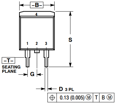
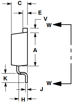
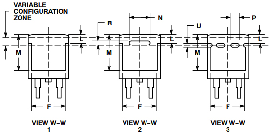
MTB30P06VT4G Package

The following diagrams show the MTB30P06VT4G Package.

View A


View B


View C

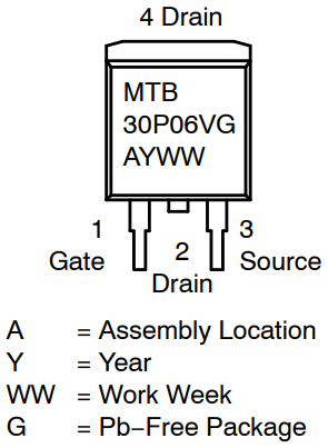
MTB30P06VT4G Marking Diagram

The following diagram shows the MTB30P06VT4G Marking Diagram.

Marking Diagram

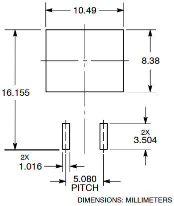
MTB30P06VT4G Soldering Footprint

The following is the Soldering Footprint of MTB30P06VT4G.

Soldering Footprint

MTB30P06VT4G Manufacturer

ON Semiconductor (Nasdaq: ON) is driving energy efficient innovations, empowering customers to reduce global energy use. The company offers a comprehensive portfolio of energy efficient power and signal management, logic, discrete and custom solutions to help design engineers solve their unique design challenges in automotive, communications, computing, consumer, industrial, LED lighting, medical, military/aerospace and power supply applications. ON Semiconductor operates a responsive, reliable, world-class supply chain and quality program, and a network of manufacturing facilities, sales offices and design centers in key markets throughout North America, Europe, and the Asia Pacific regions.


Datasheet PDF

Download datasheets and manufacturer documentation for ON Semiconductor MTB30P06VT4G.

MTB30P06VT4G Documents

Download datasheets and manufacturer documentation for MTB30P06VT4G

Frequently Asked Questions

How many pins of SP335?
3 Pins.
What’s the operating temperature of SP335?
-55°C~175°C TJ.
What is the essential property of the MTB30P06VT4G?
The MTB30P06VT4G Power MOSFET is designed to withstand high energy in the avalanche and commutation modes.
What modes is the Power MOSFET designed to withstand high energy?
Avalanche and commutation.
What is the Power MOSFET particularly well suited for?
Bridge circuits.
What is a MOSFET used for?
The MOSFET (Metal Oxide Semiconductor Field Effect Transistor) transistor is a semiconductor device which is widely used for switching and amplifying electronic signals in the electronic devices. The MOSFET is a three terminal device such as source, gate, and drain.
What is MOSFET and how it works?
A metal–oxide–semiconductor field-effect transistor (MOSFET, MOS-FET, or MOS FET) is a field-effect transistor (FET with an insulated gate) where the voltage determines the conductivity of the device. It is used for switching or amplifying signals.
What is the difference between MOSFET and transistor?
The Bipolar Junction Transistor (BJT) is a current-driven device (in contrast, MOSFET is voltage-driven) that is widely used as an amplifier, oscillator, or switch, amongst other things. A BJT has three pins – the base, collector, and emitter – and two junctions: a p-junction and n-junction.
FAQ
How many pins of SP335?
3 Pins.
What’s the operating temperature of SP335?
-55°C~175°C TJ.
What is the essential property of the MTB30P06VT4G?
The MTB30P06VT4G Power MOSFET is designed to withstand high energy in the avalanche and commutation modes.
What modes is the Power MOSFET designed to withstand high energy?
Avalanche and commutation.
What is the Power MOSFET particularly well suited for?
Bridge circuits.
What is a MOSFET used for?
The MOSFET (Metal Oxide Semiconductor Field Effect Transistor) transistor is a semiconductor device which is widely used for switching and amplifying electronic signals in the electronic devices. The MOSFET is a three terminal device such as source, gate, and drain.
What is MOSFET and how it works?
A metal–oxide–semiconductor field-effect transistor (MOSFET, MOS-FET, or MOS FET) is a field-effect transistor (FET with an insulated gate) where the voltage determines the conductivity of the device. It is used for switching or amplifying signals.
What is the difference between MOSFET and transistor?
The Bipolar Junction Transistor (BJT) is a current-driven device (in contrast, MOSFET is voltage-driven) that is widely used as an amplifier, oscillator, or switch, amongst other things. A BJT has three pins – the base, collector, and emitter – and two junctions: a p-junction and n-junction.

TAGS

Share