
MX25R1635FZUIL0 is a 16Mb Serial NOR Flash memory with an internal configuration of 2,097,152 x 8. This article mainly introduces features, pinout, datasheet and other detailed information about Macronix MX25R1635FZUIL0.
MX25R1635FZUIL0 Flash Memory: Features, Pinout, and Datasheet
IC FLASH 16M SPI 33MHZ 8USON MX25R1635FZUIL0 is a 16Mb Serial NOR Flash memory with an internal configuration of 2,097,152 x 8.
115
Jan 25, 2022
Emily Grey
MX25R1635FZUIL0
36000In Stock
Min.: 1 Mult.: 1
| Quantity | Unit Price | Ext. Price |
|---|---|---|
| 1+ | $15.7145 | $15.71 |
| 10+ | $14.825 | $148.25 |
| 100+ | $13.9858 | $1398.58 |
| 500+ | $13.1942 | $6597.1 |
| 1000+ | $12.4473 | $12447.3 |
Unit Price:$15.7145
Subtotal: $15.71
Quick Links
MX25R1635FZUIL0 Description
MX25R1635FZUIL0 is a 16Mb Serial NOR Flash memory with an internal configuration of 2,097,152 x 8. The structure becomes 4,194,304 bits x 4 or 8,388,608 bits x 2 when it is in four I/O modes. In single I/O mode, the MX25R1635FZUIL0 has a serial peripheral interface and software protocol that allows it to operate on a basic 3-wire bus.
A clock input (SCLK), a serial data input (SI), and a serial data output (SDO) are the three bus signals (SO). CS# input allows serial access to the device.
The SI and SO pins become SIO0 and SIO1 pins for address/dummy bits input and data output when it is in two I/O read modes. The SI pin, SO pin, WP# pin, and RESET#/HOLD# pin become SIO0 pin, SIO1 pin, SIO2 pin, and SIO3 pin for address/dummy bits input and data output when it is in four I/O read mode.
On the full chip, the MX25R1635FZUIL0 MXSMIO® (Serial Multi I/O) supports sequential read operation. After issuing the program/erase command, auto program/erase algorithms will be executed, which will program/erase and validate the given page, sector, or block locations. The program command is carried out on a byte, page (256 bytes), or word basis. The Erase command can be used to erase a 4K-byte sector, a 32KB block (32K-byte), a 64K-byte block, or the entire chip. A status register is included to improve user convenience by indicating the chip's status. The status read command can be used to determine whether a program or erase operation is complete using the WIP bit.
MX25R1635FZUIL0 Pinout
The following shows MX25R1635FZUIL0 Pinout.
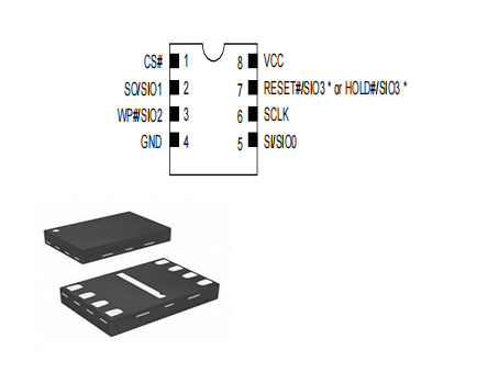
Pinout
| Pin Number | Pin Name | Description |
| 1 | CS# | Chip Select |
| 5 | SI/SIO0 | Serial Data Input (for 1 x I/O)/ Serial Data Input & Output (for 4xI/O read mode) |
| 2 | SO/SIO1 | Serial Data Output (for 1 x I/O)/ Serial Data Input & Output (for 4xI/O read mode) |
| 6 | SCLK | Clock Input |
| 3 | WP#/SIO2 | Write Protection Active Low or Serial Data Input & Output (for 4xI/O read mode) |
| 7 | RESET#/SIO3 * | Hardware Reset Pin Active low or Serial Data Input & Output (for 4xI/O read mode) |
| 7 | HOLD#/SIO3 * | To pause the device without deselecting the device or Serial Data Input & Output (for 4xI/O read mode) |
| 8 | VCC | Power Supply |
| 4 | GND | Ground |
MX25R1635FZUIL0 CAD Model
The followings are MX25R1635FZUIL0 Footprint and 3D Model.
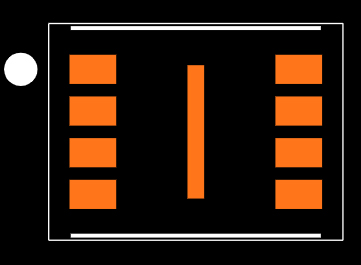
Footprint
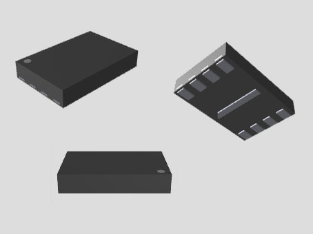
3D Model
MX25R1635FZUIL0 Features
• Ultra-Low Power Mode and High-Performance Mode
• Wide Range VCC 1.65V-3.6V for Read, Erase and Program Operations
• Unique ID and Secure OTP Support
• Multi I/O Support - Single I/O, Dual I/O and Quad I/O
• Program Suspend/Resume & Erase Suspend/Resume
Specifications
Macronix MX25R1635FZUIL0 technical specifications, attributes, parameters and parts with similar specifications to Macronix MX25R1635FZUIL0.
MX25R1635FZUIL0 Tech Specifications
MX25R1635FZUIL0 Tech Specifications
Macronix MX25R1635FZUIL0 technical specifications, attributes, parameters and parts with similar specifications to Macronix MX25R1635FZUIL0.
| Product Attribute | Attribute Value | |
|---|---|---|
| Factory Lead Time | 10 Weeks | |
| Mounting Type | Surface Mount | |
| Package / Case | 8-UFDFN Exposed Pad | |
| Surface Mount | YES | |
| Memory Types | Non-Volatile | |
| Operating Temperature | -40°C~85°C TA | |
| Packaging | Cut Tape (CT) | |
| Series | MXSMIO™ | |
| Part Status | Active | |
| Moisture Sensitivity Level (MSL) | 3 (168 Hours) | |
| Number of Terminations | 8Terminations | |
| Additional Feature | IT IS ALSO CONFIGURED AS 16M X 1 | |
| Voltage - Supply | 1.8V |
| Product Attribute | Attribute Value | |
|---|---|---|
| Terminal Position | DUAL | |
| Peak Reflow Temperature (Cel) | NOT SPECIFIED | |
| Number of Functions | 1Function | |
| Terminal Pitch | 0.5mm | |
| Time@Peak Reflow Temperature-Max (s) | NOT SPECIFIED | |
| JESD-30 Code | R-PDSO-N8 | |
| Memory Size | 16Mb 2M x 8 | |
| Operating Mode | SYNCHRONOUS | |
| Clock Frequency | 33MHz | |
| Memory Format | FLASH | |
| Memory Interface | SPI | |
| Organization | 4MX4 | |
| Memory Width | 4 |
| Product Attribute | Attribute Value | |
|---|---|---|
| Write Cycle Time - Word, Page | 100μs, 10ms | |
| Memory Density | 16777216 bit | |
| Parallel/Serial | SERIAL | |
| Programming Voltage | 3V | |
| Alternate Memory Width | 2 | |
| Voltage - Supply (Max) | 3.6V | |
| Voltage - Supply (Min) | 1.65V | |
| Length | 3mm | |
| Height Seated (Max) | 0.6mm | |
| Width | 2mm | |
| RoHS Status | ROHS3 Compliant | |
| Lead Free | Lead Free |
MX25R1635FZUIL0 Functional Block Diagram
The MX25R1635FZUIL0 Functional Block Diagram is shown as follows.
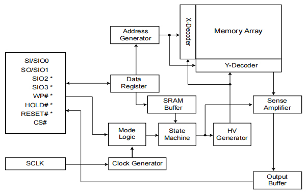
Functional Block Diagram
MX25R1635FZUIL0 Part Name Description
The MX25R1635FZUIL0 Part Name Description is shown as follows.
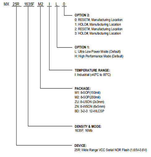
Part Name Description
MX25R1635FZUIL0 Package
The following figure is MX25R1635FZUIL0 Package.
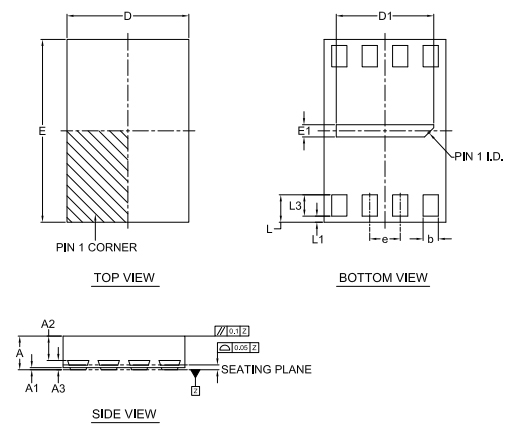
Package
MX25R1635FZUIL0 Manufacturer
Macronix, a prominent non-volatile memory (NVM) integrated device maker, offers a full range of NOR Flash, NAND Flash, and ROM solutions. Macronix continues to provide high-quality, innovative, and performance-driven products to its clients in the consumer, communication, computer, automotive, networking, and other segment markets, thanks to its world-class R&D and manufacturing capabilities.
Datasheet PDF
Download datasheets and manufacturer documentation for Macronix MX25R1635FZUIL0.
MX25R1635FZUIL0 Documents
MX25R1635FZUIL0 Documents
Download datasheets and manufacturer documentation for MX25R1635FZUIL0
PCN Packaging
TR/Tray/Tube Box Dim Chg 23/May/2017
Datasheets
MX25R1635F
Frequently Asked Questions
What is flash memory and how does it work?
Flash memory is a type of erasable read-only memory (EEPROM) that clears and rewrites data in chunks for fast, energy-efficient access and rewriting. Flash memory, or flash storage, is non-volatile, which means it remains viable even without an active power source.
Why is it called a flash memory?
Fujio Masuoka is credited with the invention of flash memory when he worked for Toshiba in the 1980s. Masuoka's colleague, Shoji Ariizumi, reportedly coined the term flash because the process of erasing all the data from a semiconductor chip reminded him of the flash of a camera.
What does the MX25R1635FZUIL0 operate on?
A basic 3-wire bus.
What is the name of the three bus signals?
A clock input.
What do the SI and SO pins become SIO0 and SIO1 pins for when it is in two I/O read modes?
Address/dummy bits input and data output.
What input allows serial access to the device?
CS#.
What does the MXSMIO® (Serial Multi I/O) support?
Sequential read operation.
What will be executed after issuing the program/erase command?
Auto program/erase algorithms.
What can be used to erase a 4K-byte sector?
The Erase command.
What is included to improve user convenience by indicating the chips status?
A status register.
The status read command can be used to determine whether a program or erase operation is complete using what?
The WIP bit.
FAQ
What is flash memory and how does it work?
Flash memory is a type of erasable read-only memory (EEPROM) that clears and rewrites data in chunks for fast, energy-efficient access and rewriting. Flash memory, or flash storage, is non-volatile, which means it remains viable even without an active power source.
Why is it called a flash memory?
Fujio Masuoka is credited with the invention of flash memory when he worked for Toshiba in the 1980s. Masuoka's colleague, Shoji Ariizumi, reportedly coined the term flash because the process of erasing all the data from a semiconductor chip reminded him of the flash of a camera.
What does the MX25R1635FZUIL0 operate on?
A basic 3-wire bus.
What is the name of the three bus signals?
A clock input.
What do the SI and SO pins become SIO0 and SIO1 pins for when it is in two I/O read modes?
Address/dummy bits input and data output.
What input allows serial access to the device?
CS#.
What does the MXSMIO® (Serial Multi I/O) support?
Sequential read operation.
What will be executed after issuing the program/erase command?
Auto program/erase algorithms.
What can be used to erase a 4K-byte sector?
The Erase command.
What is included to improve user convenience by indicating the chips status?
A status register.
The status read command can be used to determine whether a program or erase operation is complete using what?
The WIP bit.
TAGS
Comments