
MX25V1635FM1I is a 16Mb Serial NOR Flash memory with an internal configuration of 2,097,152 x 8. This article mainly introduces Features, Pinout, Datasheet and other detailed information about Macronix MX25V1635FM1I.
MX25V1635FM1I Flash Memory: Features, Pinout, and Datasheet
IC FLASH 16M SPI 80MHZ 8SOP MX25V1635FM1I is a 16Mb Serial NOR Flash memory with an internal configuration of 2,097,152 x 8. This article mainly introduces Features, Pinout,
174
Feb 24, 2022
Lena Stella
MX25V1635FM1I
922In Stock
Min.: 1 Mult.: 1
Quick Links
MX25V1635FM1I Description
MX25V1635FM1I is a 16MB Serial NOR Flash memory with a 2,097,152 x 8 internal layout. When in four I/O modes, the structure becomes 4,194,304 bits x 4 or 8,388,608 bits x 2.
The MX25V1635FM1I has a serial peripheral interface and software protocol that allows it to operate on a basic 3-wire bus when used in a single I/O mode. The three bus signals are a clock input (SCLK), a serial data input (SI), and a serial data output (SDO) (SO). The device can be accessed serially via the CS# input.
When in two I/O read modes, the SI and SO pins become SIO0 and SIO1 for address/dummy bits input and data output, respectively. When it is in four I/O read modes, the SI pin, SO pin, WP# pin, and HOLD# pin become SIO0 pin, SIO1 pin, SIO2 pin, and SIO3 pin for address/dummy bits input and data output.
On the full chip, the MX25V1635F MXSMIO® (Serial Multi I/O) allows sequential read operation.
Following the program/erase command, auto program/erase algorithms will program/erase and validate the specified page, sector, or block locations. Program commands are executed on a byte, page (256 bytes), or word basis. A 4K-byte sector, a 32KB block (32K-byte), a 64K-byte block, or an entire chip can all be erased with the Erase command.
By showing the chip state, a status register is constructed to provide the user with ease of interaction. The WIP bit can be used to determine whether a program is complete or if an erase operation is in the process using the status read command.
Advanced security features improve the protection and security functions; for more information, read the security features section.
Macronix 's unique memory cell is used in the MX25V1635FM1I, which dependably maintains memory contents even after 100,000 programs and erase cycles.
MX25V1635FM1I Pinout
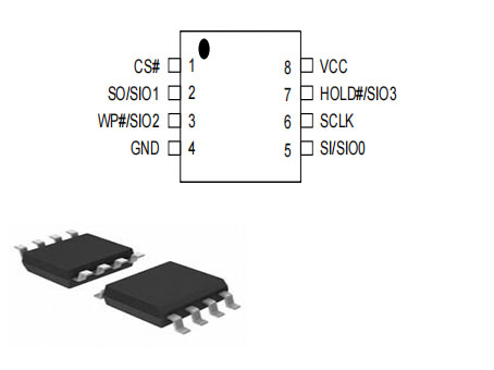
The following figure is MX25V1635FM1I Pinout.
Pinout
| Pin Number | Pin Name | Description |
| 1 | CS# | Chip Select |
| 5 | SI/SIO0 | Serial Data Input (for 1 x I/O)/ Serial Data Input & Output (for 4xI/O read mode) |
| 2 | SO/SIO1 | Serial Data Output (for 1 x I/O)/ Serial Data Input & Output (for 4xI/O read mode) |
| 6 | SCLK | Clock Input |
| 3 | WP#/SIO2 | Write Protection Active Low or Serial Data Input & Output (for 4xI/O read mode) |
| 7 | HOLD#/SIO3 | To pause the device without deselecting the device or Serial Data Input & Output (for 4xI/O read mode) |
| 8 | VCC | Power Supply |
| 4 | GND | Ground |
MX25V1635FM1I CAD Model
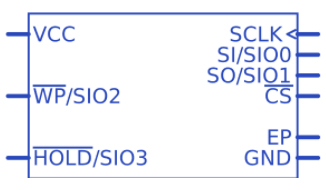
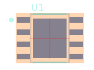
The followings are MX25V1635FM1I Symbol and Footprint.
Symbol
Footprint
MX25V1635FM1I Features
General
• Supports Serial Peripheral Interface -- Mode 0 and Mode 3
• 16,777,216 x 1 bit structure
or 8,388,608 x 2 bits (two I/O mode) structure
or 4,194,304 x 4 bits (four I/O mode) structure
• Equal Sectors with 4K byte each, Equal Blocks with 32K byte each, or Equal Blocks with 64K byte each
- Any Block can be erased individually
• Single Power Supply Operation
- Operation Voltage: 2.3V-3.6V for Read, Erase and Program Operations
• Latch-up protected to 100mA from -1V to Vcc +1V
Performance
• High Performance
- Fast read
- 1 I/O: 80MHz with 8 dummy cycles
- 2 I/O: 80MHz with 4 dummy cycles, equivalent to 160MHz
- 4 I/O: 80MHz with 2+4 dummy cycles, equivalent to 320MHz
- Fast program and erase time
- 8/16/32/64 byte Wrap-Around Burst Read Mode
• Low Power Consumption
• Minimum 100,000 erase/program cycles
• 20 years data retention
Software Features
• Input Data Format
- 1-byte Command code
• Advanced Security Features
- Block lock protection
The BP0-BP3 status bit defines the size of the area to be software protection against program and erase instructions
• Additional 8K bits secured OTP
- Features unique identifier.
- Factory locked identifiable and customer lockable
• Auto Erase and Auto Program Algorithm
- Automatically erases and verifies data at selected sector or block
- Automatically programs and verifies data at selected page by an internal algorithm that automatically times the program pulse widths (Any page to be programed should have page in the erased state first)
• Status Register Feature
• Command Reset
• Program/Erase Suspend and Program/Erase Resume
• Electronic Identification
- JEDEC 1-byte manufacturer ID and 2-byte device ID
- RES command for 1-byte Device ID
- REMS command for 1-byte manufacturer ID and 1-byte device ID
• Support Serial Flash Discoverable Parameters (SFDP) mode
• Support Unique ID (Please contact local Macronix sales for detail information)
Hardware Features
• SCLK Input
- Serial clock input
• SI/SIO0
- Serial Data Input or Serial Data Input/Output for 2 x I/O read mode and 4 x I/O read mode
• SO/SIO1
- Serial Data Output or Serial Data Input/Output for 2 x I/O read mode and 4 x I/O read mode
• WP#/SIO2
- Hardware write protection or serial data Input/Output for 4 x I/O read mode
• HOLD#/SIO3
- HOLD feature, to pause the device without deselecting the device or Serial input & Output for 4 x I/O read mode
• PACKAGE
- 8-pin SOP (150mil/200mil)
- 8-land WSON (6x5mm)
- 8-land USON (4x3mm)
- 8-land USON (2x3mm)
- 24 ball TFBGA (6x8mm)
- All devices are RoHS Compliant and Halogen -free
Specifications
MX25V1635FM1I Tech Specifications
MX25V1635FM1I Tech Specifications
Macronix MX25V1635FM1I technical specifications, attributes, parameters and parts with similar specifications to Macronix MX25V1635FM1I.
| Product Attribute | Attribute Value | |
|---|---|---|
| Factory Lead Time | 10 Weeks | |
| Surface Mount | YES | |
| Package / Case | 8-SOIC (0.154, 3.90mm Width) | |
| Mounting Type | Surface Mount | |
| Memory Types | Non-Volatile | |
| Published | 2017 | |
| Series | MXSMIO™ | |
| Packaging | Tube | |
| Operating Temperature | -40°C~85°C TA | |
| Pbfree Code | yes | |
| Part Status | Active | |
| Moisture Sensitivity Level (MSL) | 3 (168 Hours) | |
| Number of Terminations | 8Terminations | |
| Additional Feature | ALSO IT CAN BE CONFIGURED AS 16M X 1 BIT |
| Product Attribute | Attribute Value | |
|---|---|---|
| Voltage - Supply | 2.3V~3.6V | |
| Terminal Position | DUAL | |
| Peak Reflow Temperature (Cel) | NOT SPECIFIED | |
| Number of Functions | 1Function | |
| Terminal Pitch | 1.27mm | |
| Time@Peak Reflow Temperature-Max (s) | NOT SPECIFIED | |
| JESD-30 Code | R-PDSO-G8 | |
| Interface | SPI, Serial | |
| Memory Size | 16Mb 2M x 8 | |
| Operating Mode | SYNCHRONOUS | |
| Clock Frequency | 80MHz | |
| Memory Format | FLASH | |
| Memory Interface | SPI | |
| Organization | 4MX4 |
| Product Attribute | Attribute Value | |
|---|---|---|
| Memory Width | 4 | |
| Write Cycle Time - Word, Page | 100μs, 4ms | |
| Memory Density | 16777216 bit | |
| Programming Voltage | 3V | |
| Alternate Memory Width | 2 | |
| Voltage - Supply (Max) | 3.6V | |
| Voltage - Supply (Min) | 2.3V | |
| Width | 3.9mm | |
| Height Seated (Max) | 1.75mm | |
| Length | 4.9mm | |
| RoHS Status | ROHS3 Compliant | |
| Lead Free | Lead Free |
MX25V1635FM1I Functional Block Diagram
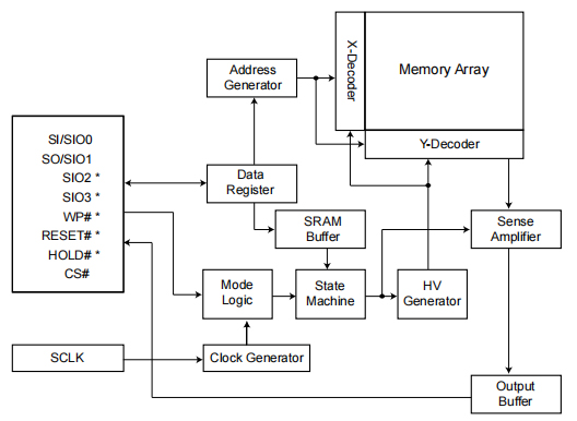
The following figure is MX25V1635FM1I Functional Block Diagram.
Functional Block Diagram
MX25V1635FM1I Part Name Description
The following figure shows MX25V1635FM1I Part Name Description.
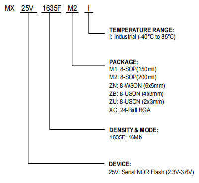
Part Name Description
MX25V1635FM1I Package
The following figure is MX25V1635FM1I Package.
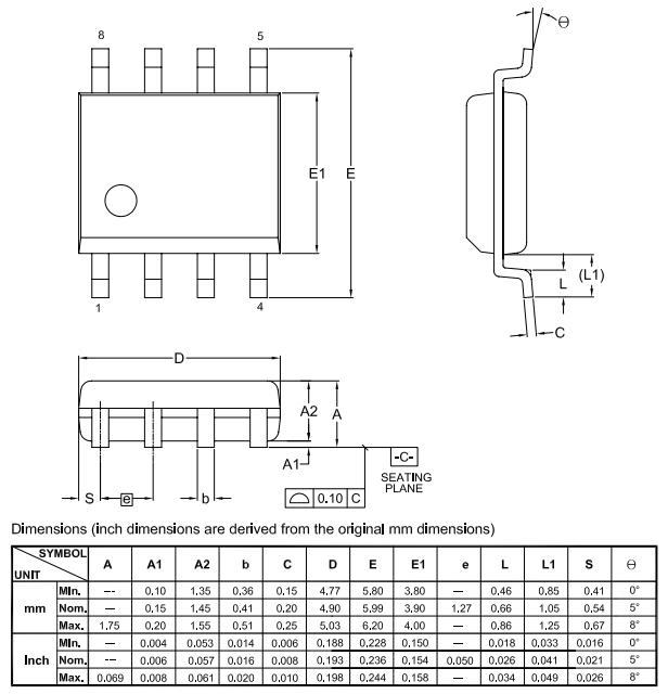
Package
MX25V1635FM1I Manufacturer
Macronix, a prominent non-volatile memory (NVM) integrated device maker, offers a full range of NOR Flash, NAND Flash, and ROM solutions. Macronix continues to provide high-quality, innovative, and performance-driven products to its clients in the consumer, communication, computer, automotive, networking, and other segment markets, thanks to its world-class R&D and manufacturing capabilities.
Datasheet PDF
MX25V1635FM1I Documents
MX25V1635FM1I Documents
Download datasheets and manufacturer documentation for MX25V1635FM1I
PCN Packaging
TR/Tray/Tube Box Dim Chg 23/May/2017
Frequently Asked Questions
What is flash memory examples?
Flash memory is widely used with car radios, cell phones, digital cameras, PDAs, solid-state drives, tablets, and printers. The picture is an example of different flash memory. For additional information and examples of flash memory cards, see our flash memory card page.
Is flash memory the same as RAM?
Flash memory is used primarily for storage, while RAM (random access memory) performs calculations on the data retrieved from storage. By their nature, flash memory and RAM are faster than storage alternatives, such as hard disk and tape.
What is flash memory and how does it work?
Flash memory is a type of erasable read-only memory (EEPROM) that clears and rewrites data in chunks for fast, energy-efficient access and rewriting. Flash memory, or flash storage, is non-volatile, which means it remains viable even without an active power source.
What does the MX25V1635FM1I operate on when used in a single I/O mode?
A basic 3-wire bus.
What do the SI and SO pins become when in two I/O read modes?
SIO0 and SIO1.
How many I/O read modes is the MX25V1635FM1I?
Four.
What does the MX25V1635F MXSMIO® allow on the full chip?
Sequential read operation.
What command does the MX25V1635F MXSMIO® (Serial Multi I/O) allow sequential read operation?
Program/erase.
What type of block can be erased with the Erase command?
64K-byte.
What is constructed to provide the user with ease of interaction?
A status register.
What can be used to determine whether a program is complete or if an erase operation is in the process using the status read command?
The WIP bit.
What improves the protection and security functions?
Advanced security features.
FAQ
What is flash memory examples?
Flash memory is widely used with car radios, cell phones, digital cameras, PDAs, solid-state drives, tablets, and printers. The picture is an example of different flash memory. For additional information and examples of flash memory cards, see our flash memory card page.
Is flash memory the same as RAM?
Flash memory is used primarily for storage, while RAM (random access memory) performs calculations on the data retrieved from storage. By their nature, flash memory and RAM are faster than storage alternatives, such as hard disk and tape.
What is flash memory and how does it work?
Flash memory is a type of erasable read-only memory (EEPROM) that clears and rewrites data in chunks for fast, energy-efficient access and rewriting. Flash memory, or flash storage, is non-volatile, which means it remains viable even without an active power source.
What does the MX25V1635FM1I operate on when used in a single I/O mode?
A basic 3-wire bus.
What do the SI and SO pins become when in two I/O read modes?
SIO0 and SIO1.
How many I/O read modes is the MX25V1635FM1I?
Four.
What does the MX25V1635F MXSMIO® allow on the full chip?
Sequential read operation.
What command does the MX25V1635F MXSMIO® (Serial Multi I/O) allow sequential read operation?
Program/erase.
What type of block can be erased with the Erase command?
64K-byte.
What is constructed to provide the user with ease of interaction?
A status register.
What can be used to determine whether a program is complete or if an erase operation is in the process using the status read command?
The WIP bit.
What improves the protection and security functions?
Advanced security features.
TAGS
Comments