ATTENTION: Due to increased demand and order volume, processing time may take an additional 1-3 business days.
HomeCommunitySubjectPCA9555 CMOS Device: Datasheet, Pinout, Application Circuit

PCA9555 CMOS Device: Datasheet, Pinout, Application Circuit

NXP PCA9555PW,118 I/O Expander, 16bit, 400 kHz, I2C, SMBus, 2.3 V, 5.5 V, TSSOP The PCA9555 is a 24-pin CMOS device, and this post mainly covers its pinout, datasheet, application and more details, furthermore, there is a huge range of Semiconductors, Capacitors, Resistors and ICs in stock. Welcome RFQ.
167

Sep 26, 2021

Sylvia Terry

PCA9555 32-Bit GPIO Expander with Arduino


NXP PCA9555PW,118 I/O Expander, 16bit, 400 kHz, I2C, SMBus, 2.3 V, 5.5 V, TSSOP

The PCA9555 is a 24-pin CMOS device, and this post mainly covers its pinout, datasheet, application and more details, furthermore, there is a huge range of Semiconductors, Capacitors, Resistors and ICs in stock. Welcome RFQ.
 

PCA9555PW,118

5000In Stock
Min.: 1 Mult.: 1
Quantity Unit Price Ext. Price
1+ $1.80701$1.81
10+ $1.70472$17.05
100+ $1.60823$160.82
500+ $1.5172$758.6
1000+ $1.43132$1431.32
Unit Price:$1.80701
Subtotal: $1.81
Looking for a better price? Want a lower wholesale price? Please send an RFQ, and we will respond immediately.
Quick Links

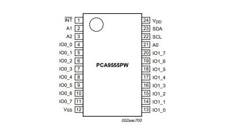
PCA9555 Pinout

PCA9555 Pinout

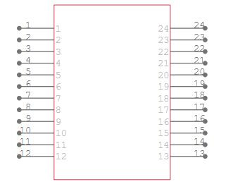
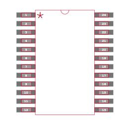
PCA9555 CAD Model

PCA9555 Symbol


PCA9555 Footprint


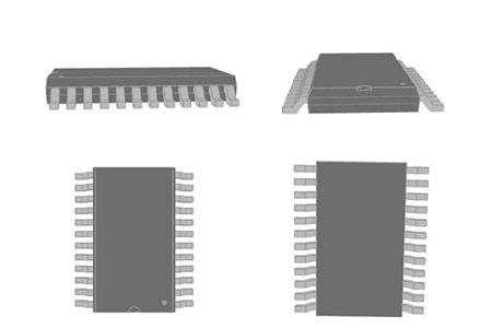
PCA9555 3D Model

What is PCA9555?

The PCA9555 is a 24-pin CMOS device that provides 16 bits of General Purpose parallel Input/Output (GPIO) expansion for I2C-bus/SMBus applications and was developed to enhance the NXP Semiconductors family of I2C-bus I/O expanders.

The PCA9555 consists of two 8-bit Configuration (Input or Output selection); Input, Output and Polarity Inversion (active HIGH or active LOW operation) registers. The system master can enable the I/Os as either inputs or outputs by writing to the I/O configuration bits.

The PCA9555 open-drain interrupt output is activated when any input state differs from its corresponding input port register state and is used to indicate to the system master that an input state has changed. The power-on reset sets the registers to their default values and initializes the device state machine.


Specifications

NXP USA Inc. PCA9555PW,118 technical specifications, attributes, parameters and parts with similar specifications to NXP USA Inc. PCA9555PW,118.

PCA9555PW,118 Tech Specifications

NXP USA Inc. PCA9555PW,118 technical specifications, attributes, parameters and parts with similar specifications to NXP USA Inc. PCA9555PW,118.

Product Attribute Attribute Value
Factory Lead Time7 Weeks
Mounting TypeSurface Mount
Package / Case24-TSSOP (0.173, 4.40mm Width)
Surface MountYES
Number of I/Os16I/Os
Operating Temperature-40°C~85°C
PackagingTape & Reel (TR)
Published2003
JESD-609 Codee4
Part StatusActive
Moisture Sensitivity Level (MSL)1 (Unlimited)
Number of Terminations24Terminations
Terminal FinishNickel/Palladium/Gold (Ni/Pd/Au)
Product Attribute Attribute Value
HTS Code8542.39.00.01
Voltage - Supply2.3V~5.5V
Terminal PositionDUAL
Terminal FormGULL WING
Peak Reflow Temperature (Cel)260
Supply Voltage3V
Terminal Pitch0.65mm
Time@Peak Reflow Temperature-Max (s)30
Base Part NumberPCA9555
Pin Count24
JESD-30 CodeR-PDSO-G24
Qualification StatusNot Qualified
Output TypePush-Pull
Product Attribute Attribute Value
Power Supplies2.5/5V
InterfaceI2C, SMBus
Number of Ports2Ports
Number of Bits16Bits
Clock Frequency400kHz
Interrupt OutputYes
Current - Output Source/Sink10mA 25mA
FeaturesPOR
Length7.8mm
Height Seated (Max)1.1mm
Width4.4mm
RoHS StatusROHS3 Compliant
0 Products View Similar

PCA9555 Feature

■ Operating power supply voltage range of 2.3 V to 5.5 V

■ 5 V tolerant I/Os

■ Polarity Inversion register

■ The active LOW interrupt output

■ Low standby current

■ Noise filter on SCL/SDA inputs

■ No glitch on power-up

■ Internal power-on reset

■ 16 I/O pins which default to 16 inputs

■ 0 Hz to 400 kHz clock frequency

■ ESD protection exceeds 2000 V HBM per JESD22-A114, 200 V MM per JESD22-A115, and 1000 V CDM per JESD22-C101

■ Latch-up testing is done to JEDEC Standard JESD78 which exceeds 100 mA

■ Six packages offered: DIP24, SO24, SSOP24, TSSOP24, HVQFN24 and HWQFN2

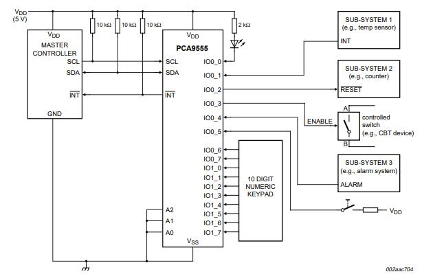
PCA9555 Typical Application Circuit

The typical application circuit for PCA9555 is shown below.

PCA9555 Typical Application Circuit

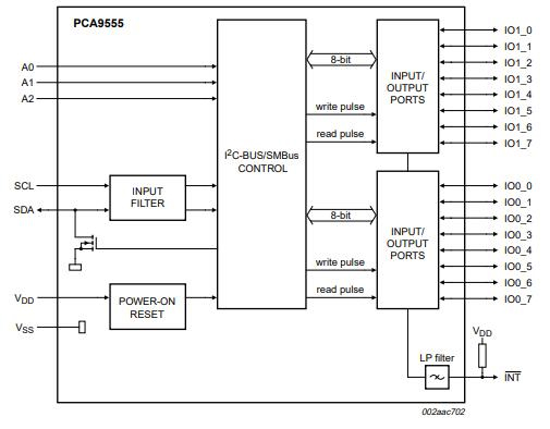
PCA9555 Block Diagram

PCA9555 Block Diagram

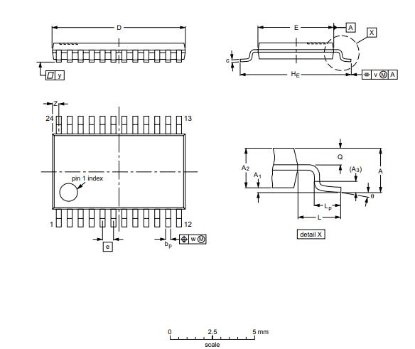
PCA9555 Package

Note:  Other packages of  PCA9555  can be taken from the datasheet below.

PCA9555 Manufacturer

NXP Semiconductors is dedicated to providing secure connectivity solutions for embedded applications, the company has 45,000 employees in more than 35 countries. and has been operating, with its experience and expertise, for more than 60 years. As a leader in this field, NXP is driving innovation in the secure connected vehicle, end-to-end security & privacy and smart connected solutions markets, with the hope of making lives easier, better and safer Freescale Semiconductor parts are now a part of the NXP family.

Datasheet PDF

Download datasheets and manufacturer documentation for NXP USA Inc. PCA9555PW,118.

PCA9555PW,118 Documents

Download datasheets and manufacturer documentation for PCA9555PW,118

Frequently Asked Questions

How many package does PCA9555 offer?
It offered 6 packages: DIP24, SO24, SSOP24, TSSOP24, HVQFN24 and HWQFN2.
What is the operating power supply voltage of PCA9555?
Operating power supply voltage range of 2.3 V to 5.5 V.
What about the clock frequency of PCA9555?
It is a 0 Hz to 400 kHz clock frequency.
FAQ
How many package does PCA9555 offer?
It offered 6 packages: DIP24, SO24, SSOP24, TSSOP24, HVQFN24 and HWQFN2.
What is the operating power supply voltage of PCA9555?
Operating power supply voltage range of 2.3 V to 5.5 V.
What about the clock frequency of PCA9555?
It is a 0 Hz to 400 kHz clock frequency.

TAGS

Share