ATTENTION: Due to increased demand and order volume, processing time may take an additional 1-3 business days.
HomeCommunitySubjectPCF8591 A/D and D/A Converter: Datasheet, Pinout, Block Diagram

PCF8591 A/D and D/A Converter: Datasheet, Pinout, Block Diagram

PCF8591 Series 2.5 V - 6 V 8-bit A/D and D/A converter - SOIC-16 The PCF8591 is a single-chip, single-supply low-power 8-bit CMOS data acquisition device with four analogue inputs, one analogue output and a serial I2C-bus interface.

1499

Sep 18, 2021

Larry Christiana

Analog-To-Digital Converters (ADC) with Raspberry Pi (Freenove Chips PCF8591 and ADS7830)


PCF8591 Series 2.5 V - 6 V 8-bit A/D and D/A converter - SOIC-16

The PCF8591 is a single-chip, single-supply low-power 8-bit CMOS data acquisition device with four analogue inputs, one analogue output and a serial I2C-bus interface. This article will unlock its pinout, datasheet, block diagram and more details.
PCF8591T/2,518

10000In Stock
Min.: 1 Mult.: 1
Price not displayed? Not available to buy online? Please send an RFQ, and we will respond immediately.
Quick Links

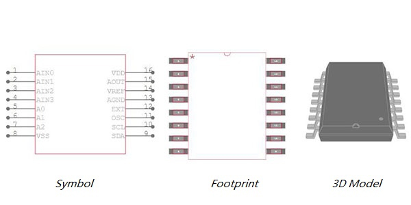
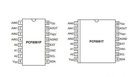
PCF8591 Pinout

PCF8591 Pinout


Pin   Number Pin Name Description
1 AINO analogue inputs (AD converter)
2 AIN1
3 AIN2
4 AIN3
5 A0 hardware slave address
6 A1
7 A2
8 Vss ground supply voltage
9 SDA I2C-bus serial data input and output
10 SCL I2C-bus serial clock input
11 OSC. oscillator input/output
12 EXT external/internal switch for oscillator input
13 AGND analogue ground supply
14 VREF voltage reference input
15 AOUT analogue output (D/A converter)
16 Voo supply voltage

Pin Description

PCF8591 Description

The PCF8591 is a single-chip, single-supply low-power 8-bit CMOS data acquisition device with four analogue inputs, one analogue output and a serial I2C-bus interface. Three address pins A0, A1 and A2 are used for programming the hardware address, allowing the use of up to eight devices connected to the I2C-bus without additional hardware. Address, control and data to and from the device are transferred serially via the two-line bidirectional I2C-bus.


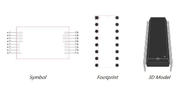
PCF8591 CAD Model

PCF8591P CAD Model

PCF8591T CAD Model

Specifications

NXP USA Inc. PCF8591T/2,518 technical specifications, attributes, parameters and parts with similar specifications to NXP USA Inc. PCF8591T/2,518.

PCF8591T/2,518 Tech Specifications

NXP USA Inc. PCF8591T/2,518 technical specifications, attributes, parameters and parts with similar specifications to NXP USA Inc. PCF8591T/2,518.

Product Attribute Attribute Value
Factory Lead Time7 Weeks
Mounting TypeSurface Mount
Package / Case16-SOIC (0.295, 7.50mm Width)
Surface MountYES
Operating Temperature-40°C~85°C
PackagingTape & Reel (TR)
Published1997
JESD-609 Codee4
Part StatusActive
Moisture Sensitivity Level (MSL)3 (168 Hours)
Number of Terminations16Terminations
TypeADC, DAC
Product Attribute Attribute Value
Terminal FinishNickel/Palladium/Gold (Ni/Pd/Au)
Voltage - Supply2.5V~6V
Terminal PositionDUAL
Terminal FormGULL WING
Peak Reflow Temperature (Cel)260
Number of Functions1Function
Supply Voltage5V
Terminal Pitch1.27mm
Time@Peak Reflow Temperature-Max (s)40
Base Part NumberPCF8591
Pin Count16
JESD-30 CodeR-PDSO-G16
Product Attribute Attribute Value
Qualification StatusNot Qualified
Supply Voltage-Max (Vsup)6V
Supply Voltage-Min (Vsup)2.5V
Number of Channels4Channels
Data InterfaceI2C, Serial
Sampling Rate (Per Second)11.1k
Voltage Supply SourceSingle Supply
Resolution (Bits)8 b
Length10.3mm
Height Seated (Max)2.65mm
Width7.5mm
RoHS StatusROHS3 Compliant
0 Products View Similar

PCF8591 Features

 Single power supply

 Operating supply voltage 2.5 V to 6.0 V

 Low standby current

 Serial input and output via I2C-bus

 I2C address selection by 3 hardware address pins

 Max sampling rate is given by I2C-bus speed

 4 analogue inputs configurable as single-ended or differential inputs

 Auto-incremented channel selection

 Analogue voltage range from VSS to VDD

 On-chip track and hold circuit

 8-bit successive approximation A/D conversion

 Multiplying DAC with one analogue output.

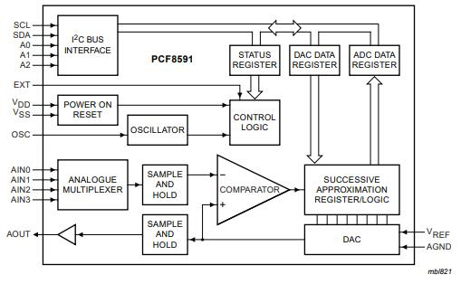
PCF8591 Block Diagram

PCF8591 Functional Block Diagram

PCF8591 Applications

 Supply monitoring

 Reference setting

 Analogue control loops

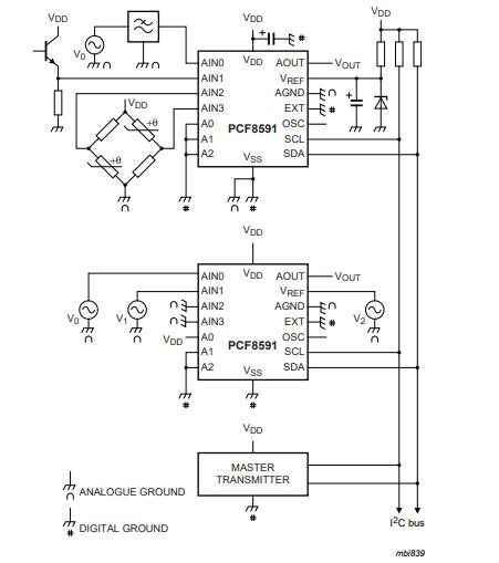
PCF8591 Application Diagram

PCF8591 Application Diagram

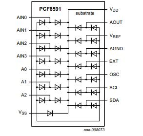
PCF8591 Internal Circuit

PCF8591 Internal Circuit

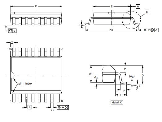
PCF8591 Package

PCF8591 DIP16 Pacakge

PCF8591 SO16 Package

PCF8591 Manufacturer

NXP Semiconductors is dedicated to providing secure connectivity solutions for embedded applications, the company has 45,000 employees in more than 35 countries. and has been operating, with its experience and expertise, for more than 60 years. As a leader in this field, NXP is driving innovation in the secure connected vehicle, end-to-end security & privacy and smart connected solutions markets, with the hope of making lives easier, better and safer Freescale Semiconductor parts are now a part of the NXP family.


Datasheet PDF

Download datasheets and manufacturer documentation for NXP USA Inc. PCF8591T/2,518.

PCF8591T/2,518 Documents

Download datasheets and manufacturer documentation for PCF8591T/2,518

Datasheets
PCF8591
Environmental Information
NXP RoHS3 Cert

Frequently Asked Questions

What is PCF8591?
The PCF8591 is a single-chip, single-supply low-power 8-bit CMOS data acquisition device with four analogue inputs, one analogue output and a serial I2C-bus interface. Three address pins A0, A1 and A2 are used for programming the hardware address, allowing the use of up to eight devices connected to the I2C-bus without additional hardware. Address, control and data to and from the device are transferred serially via the two-line bidirectional I2C-bus.
What is the function of PCF8591?
The functions of the device include analogue input multiplexing, on-chip track and hold function, 8-bit analogue-to-digital conversion and an 8-bit digital-to-analogue conversion. The maximum conversion rate is given by the maximum speed of the I2C-bus.
How do I connect my Raspberry Pi to PCF8591?
PCF8591 is an 8 bit analogue to digital or 8 bit digital to analogue converter module meaning each pin can read analogue values up to 256. ... Configuring I2C in Raspberry Pi. Scanning I2C Address of PCF8591 using Raspberry Pi. Complete python code and Video is given below.
How to package PCF8591?
It is available in 16-SOIC and 16-DIP packages.
FAQ
What is PCF8591?
The PCF8591 is a single-chip, single-supply low-power 8-bit CMOS data acquisition device with four analogue inputs, one analogue output and a serial I2C-bus interface. Three address pins A0, A1 and A2 are used for programming the hardware address, allowing the use of up to eight devices connected to the I2C-bus without additional hardware. Address, control and data to and from the device are transferred serially via the two-line bidirectional I2C-bus.
What is the function of PCF8591?
The functions of the device include analogue input multiplexing, on-chip track and hold function, 8-bit analogue-to-digital conversion and an 8-bit digital-to-analogue conversion. The maximum conversion rate is given by the maximum speed of the I2C-bus.
How do I connect my Raspberry Pi to PCF8591?
PCF8591 is an 8 bit analogue to digital or 8 bit digital to analogue converter module meaning each pin can read analogue values up to 256. ... Configuring I2C in Raspberry Pi. Scanning I2C Address of PCF8591 using Raspberry Pi. Complete python code and Video is given below.
How to package PCF8591?
It is available in 16-SOIC and 16-DIP packages.

TAGS

Share