ATTENTION: Due to increased demand and order volume, processing time may take an additional 1-3 business days.
HomeCommunitySubjectPCM5100APWR Audio Stereo DAC: Diagram, Pinout, and Datasheet

PCM5100APWR Audio Stereo DAC: Diagram, Pinout, and Datasheet

IC DAC 16/24/32BIT SRL 20TSSOP The PCM5100APWR is a 2.1 VRMS, 112/106/100 dB Audio Stereo DAC with PLL and 32-bit, 384 kHz PCM Interface. This article mainly introduces Diagram, Pinout, Datasheet and other detailed information about Texas Instruments PCM5100APWR.

177

Apr 12, 2022

Ken Josh

What is a DAC? - Explained


IC DAC 16/24/32BIT SRL 20TSSOP

The PCM5100APWR is a 2.1 VRMS, 112/106/100 dB Audio Stereo DAC with PLL and 32-bit, 384 kHz PCM Interface. This article mainly introduces Diagram, Pinout, Datasheet and other detailed information about Texas Instruments PCM5100APWR.

PCM5100APWR

32In Stock
Min.: 1 Mult.: 1
Price not displayed? Not available to buy online? Please send an RFQ, and we will respond immediately.
Quick Links

PCM5100APWR Description

The PCM5100APWR is a family of monolithic CMOS-integrated circuits in a tiny TSSOP package that includes a stereo digitalto-analog converter and accompanying support circuitry. To offer superior dynamic performance and better clock jitter tolerance, the PCM5100APWR devices leverage the latest iteration of TI's sophisticated segmentDAC architecture.

The PCM5100APWR  device produces 2.1-VRMS ground centered outputs using DirectpathTM charge-pump technology, allowing designers to avoid DC blocking capacitors on the output as well as extra muting circuits often associated with single supply line drivers.

By enabling loads as low as 1 k per pin, the integrated line driver outperforms all other chargepump-based line drivers

The device's internal PLL eliminates the need for a system clock (also known as master clock), allowing for a 3-wire  I2S  connection and lower system EMI.

For pop-free performance, the Intelligent Clock Error and PowerSense undervoltage protection use a two-level mute mechanism.

The PCM5100APWR series offers up to 20 dB lower out-of-band noise than many typical switched capacitor  DAC  architectures, decreasing EMI and aliasing in downstream amplifiers/ADCs (measured from traditional 100-kHz OBN measurements to 3 MHz).


PCM5100APWR Pinout

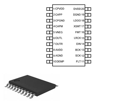
The following figure is PCM5100APWR Pinout.

Pinout


Pin Number Pin Name Description
9 AGND Analog ground
8 AVDD Analog power supply, 3.3 V
13 BCK Audio data bit clock input
4 CAPM Charge pump flying capacitor terminal for negative rail
2 CAPP Charge pump flying capacitor terminal for positive rail
3 CPGND Charge pump ground
1 CPVDD Charge pump power supply, 3.3 V
10 DEMP De-emphasis control for 44.1-kHz sampling rate(1): Off (Low) / On (High)
19 DGND Digital ground
14 DIN Audio data input
20 DVDD Digital power supply, 1.8 V or 3.3 V
11 FLT Filter select : Normal latency (Low) / Low latency (High)
16 FMT Audio format selection : I2S (Low) / Left-justified (High)
18 LDOO Internal logic supply rail terminal for decoupling, or external 1.8 V supply terminal
15 LRCK Audio data word clock input
6 OUTL Analog output from DAC left channel
7 OUTR Analog output from DAC right channel
12 SCK System clock input
5 VNEG Negative charge pump rail terminal for decoupling, –3.3 V
17 XSMT Soft mute control(1): Soft mute (Low) / soft un-mute (High)

PCM5100APWR CAD Model

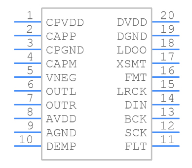
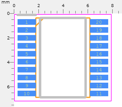
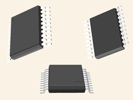
The followings are PCM5100APWR Symbol, Footprint and 3D Model.

Symbol

Footprint

3D Model

PCM5100APWR Features

• Ultra Low Out-of-Band Noise

• Integrated High-Performance Audio PLL with BCK Reference to Generate SCK Internally

• Direct Line Level 2.1-VRMS Output

• No DC Blocking Capacitors Required

• Line Level Output Down to 1KΩ

• Intelligent Muting System; Soft Up or Down Ramp and Analog Mute For 120-dB Mute SNR

• Accepts 16-, 24-, and 32-Bit Audio Data 

• PCM Data Formats: I2S, Left-Justified

• Automatic Power-Save Mode When LRCK And BCK Are Deactivated 

• 1.8 V or 3.3 V Failsafe LVCMOS Digital Inputs

• Simple Configuration Using Hardware Pins 

• Single-Supply Operation: 14

– 3.3 V Analog, 1.8 V or 3.3 V Digital

• Qualified in Accordance with AEC-Q100 

Specifications

PCM5100APWR Tech Specifications

Texas Instruments PCM5100APWR technical specifications, attributes, parameters and parts with similar specifications to Texas Instruments PCM5100APWR.

Product Attribute Attribute Value
Lifecycle StatusACTIVE (Last Updated: 4 days ago)
Factory Lead Time6 Weeks
Contact PlatingGold
MountSurface Mount
Mounting TypeSurface Mount
Package / Case20-TSSOP (0.173, 4.40mm Width)
Number of Pins20Pins
Operating Temperature-25°C~85°C
PackagingTape & Reel (TR)
SeriesDirectPath™
JESD-609 Codee4
Pbfree Codeyes
Part StatusActive
Moisture Sensitivity Level (MSL)1 (Unlimited)
Number of Terminations20Terminations
ECCN CodeEAR99
TypeDAC, Audio
Max Power Dissipation187mW
Product Attribute Attribute Value
Voltage - Supply1.65V~3.46V
Terminal PositionDUAL
Terminal FormGULL WING
Peak Reflow Temperature (Cel)260
Number of Functions1Function
Supply Voltage3.3V
Time@Peak Reflow Temperature-Max (s)NOT SPECIFIED
Base Part NumberPCM5100
Pin Count20
Qualification StatusNot Qualified
Output Voltage2.1V
Output TypeVoltage
Operating Supply Voltage3.3V
PolarityUnipolar
InterfaceI2S, Serial
Operating Supply Current9mA
Number of Bits32Bits
Supply TypeAnalog, Digital
Product Attribute Attribute Value
Data InterfacePCM
Sampling Rate384 ksps
Sampling Rate (Per Second)384k
Power Consumption59.4mW
Input Bit CodeBINARY
Conversion Rate384 ksps
Voltage Supply SourceAnalog Digital
Signal to Noise Ratio (SNR)100 dB
Number of ADC Channels0ADC Channel
Resolution (Bits)16 b, 24 b, 32 b
Number of DAC Channels2DAC Channels
Height1.2mm
Length6.5mm
Width4.4mm
Thickness1mm
REACH SVHCNo SVHC
RoHS StatusROHS3 Compliant
Lead FreeLead Free
0 Products View Similar

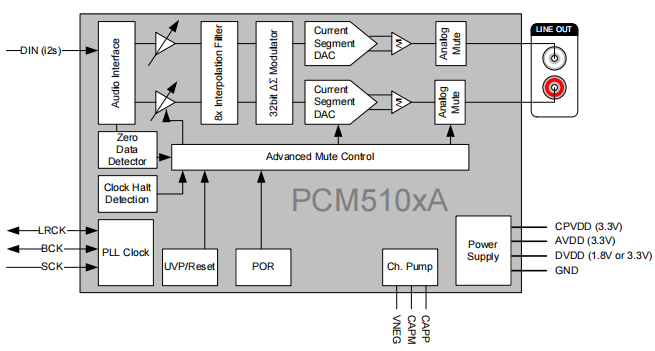
PCM5100APWR Functional Block Diagram

The PCM5100APWR Functional Block Diagram is shown as follows.

Functional Block Diagram

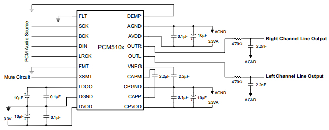
PCM5100APWR Typical Application

The PCM5100APWR Typical Application is shown as follows.

Typical Application


• Hardware control

– Normal filter latency

– I2S digital audio interface

– Power rail monitoring from the system 12-V rail to mute system power loss early

• 2.1-VRMS single-ended analog outputs

• Single 3.3-V supply

• 3-wire I2S interface (BCK PLL)


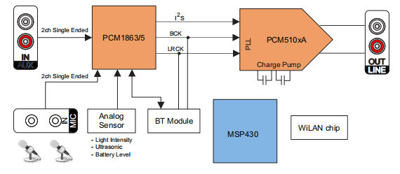
PCM5100APWR Simplified System Diagram

The PCM5100APWR Simplified System Diagram is shown as follows.

Simplified System Diagram

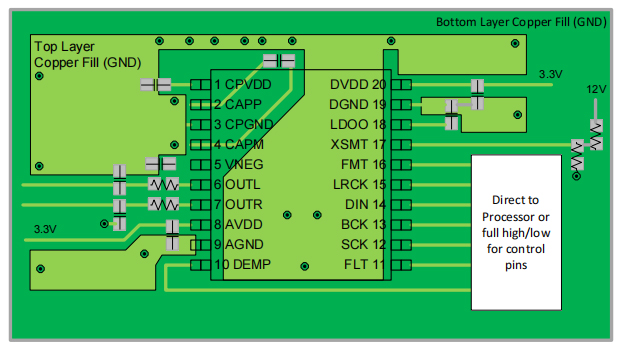
PCM5100APWR Layout

• The PCM5100APWR device family is easy to set up. For a whole device, most engineers employ a shared common ground. AGND and DGND are both connected to GND.

• For best analog performance, keep digital clock and interface traces away from analog outputs with good system partitioning. Any high-speed clock return currents influencing the analog outputs are reduced as a result.

• The power supply and charge pump decoupling capacitors should be as close to the device as practicable.

• Signal routing should be done on the top layer, whereas GND can be done on the bottom layer.

Layout

PCM5100APWR Alternatives

Part Number Description Manufacturer
PCM5100APWCONVERTERS 2VRMS DirectPath™, 100dB Audio Stereo DAC with 32-bit, 384kHz PCM Interface 20-TSSOP -25 to 85 Texas Instruments
PCM5100AQPWRQ1CONVERTERS Automotive Catalog 2VRMS DirectPath™, 100dB Audio Stereo DAC with 32-bit, 384kHz PCM Interface 20-TSSOP -40 to 125 Texas Instruments

PCM5100APWR Applications

• A/V Receivers, DVD, BD Players

• Automotive Infotainment and Telematics

• HDTV Receivers

• Aftermarket Automotive Amplifiers

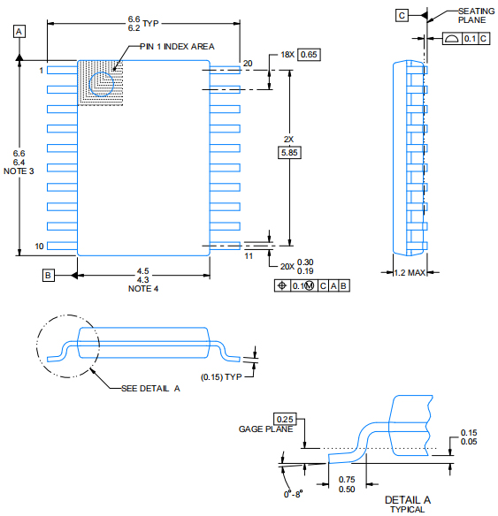
PCM5100APWR Package

The PCM5100APWR Package is shown as follows.

Package

PCM5100APWR Manufacturer

As a global semiconductor company operating in 35 countries, Texas Instruments  (TI) is first and foremost a reflection of its people. From the TIer who unveiled the first working integrated circuit in 1958 to the more than 30,000 TIers around the world today who design, manufacture and sell analog and embedded processing chips, we are problem-solvers collaborating to change the world through technology.


Datasheet PDF

PCM5100APWR Documents

Download datasheets and manufacturer documentation for PCM5100APWR

Frequently Asked Questions

What type of circuits is the PCM5100APWR?
Monolithic CMOS-integrated circuits.
What segmentDAC architecture does the PCM5100APWR use?
TI.
What technology does the PCM5100APWR use to produce ground centered outputs?
DirectpathTM charge-pump technology.
What is a system clock also known as?
Master clock.
What does the Intelligent Clock Error and PowerSense undervoltage protection use for pop-free performance?
Two-level mute mechanism.
How much lower out-of-band noise does the PCM5100APWR series offer?
20 dB.
FAQ
What type of circuits is the PCM5100APWR?
Monolithic CMOS-integrated circuits.
What segmentDAC architecture does the PCM5100APWR use?
TI.
What technology does the PCM5100APWR use to produce ground centered outputs?
DirectpathTM charge-pump technology.
What is a system clock also known as?
Master clock.
What does the Intelligent Clock Error and PowerSense undervoltage protection use for pop-free performance?
Two-level mute mechanism.
How much lower out-of-band noise does the PCM5100APWR series offer?
20 dB.

TAGS

Share