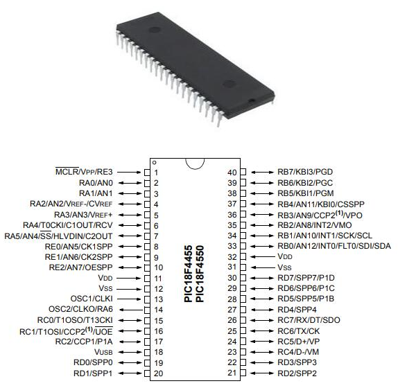
| Pin Number |
Pin Name |
Description |
| 1 |
MCLR/VPP/RE3 |
MCLR: Master Clear(RESET) Input VPP: programming voltage input RE3: I/O pin of PORTE, PIN 3 |
| 2 |
RA0/AN0 |
RA0: I/O pin of PORTA, PIN 0 AN0: Analog input 0 |
| 3 |
RA1/AN1 |
RA1: I/O pin of PORTA, PIN 1 AN1: Analog input 1 |
| 4 |
RA2/AN2/VREF-/CVREF |
RA2: I/O pin of PORTA, PIN 2 AN2: Analog input 2 VREF-: A/D reference voltage (low) input CVREF: Analog comparator reference output |
| 5 |
RA3/AN3/VREF+ |
RA3: I/O pin of PORTA, PIN 3 AN3: Analog input3 VREF+: A/D reference voltage (high) input |
| 6 |
RA4/T0CKI/C1OUT/RCV |
RA4: I/O pin of PORTA, PIN 4 T0CKI: Timer0 external clock input C1OUT: Comparator 1 output RCV: External USB transceiver RCV input |
| 7 |
RA5/AN4/SS/HLVDIN/C2OUT |
RA5: I/O pin of PORTA, PIN 5 AN4: Analog input 4 SS: SPI slave select input HLDVIN: High/Low-Voltage Detect input C2OUT: Comparator 2 output |
| 8 |
RE0/AN5/CK1SPP |
RE0: I/O pin of PORTE, PIN 0 AN5: Analog input 5 CK1SPP: SPP clock 1 output |
| 9 |
RE1/AN6/CK2SPP |
RE1: I/O pin of PORTE, PIN 1 AN6: Analog input 6 CK2SPP: SPP clock 2 output |
| 10 |
RE2/AN7/OESPP |
RE2: I/O pin of PORTE, PIN 2 AN6: Analog input 7 OESPP: SPP Enabled output |
| 11 |
VDD |
Positive Power Supply (+5V) |
| 12 |
VSS |
Ground |
| 13 |
OSC1/CLKI |
OSC1:Oscillator pin 1 CLKI: External clock source input |
| 14 |
OSC2/CLKO/RA6 |
OSC2: Oscillator pin 2 CLKO: clock source output RA6: I/O pin of PORTA, PIN 6 |
| 15 |
RC0/T1OSO/T13CKI |
RC0: I/O pin of PORTC, PIN 0 T1OSO:Timer1 oscillator output T13CKI: Timer1/Timer3 external clock input |
| 16 |
RC1/T1OSI/CCP2/UOE |
RC1: I/O pin of PORTC, PIN 1 T1OSI: Timer1 oscillator input CCP2:Capture 2 input/Compare 2 output/PWM2 output UOE: External USB transceiver OE output |
| 17 |
RC2/CCP1/P1A |
RC2: I/O pin of PORTC, PIN 2 CCP1: Capture 1 input/Compare 1 output/PWM1 output. P1A : Enhanced CCP1 PWM output, channel A |
| 18 |
VUSB |
VUSB: Internal USB 3.3V voltage regulator output |
| 19 |
RD0/SPP0 |
RD0: I/O pin of PORTD, PIN 0 SPP0: Streaming Parallel Port data |
| 20 |
RD1/SPP1 |
RD1: I/O pin of PORTD, PIN 1 SPP1: Streaming Parallel Port data |
| 21 |
RD2/SPP2 |
RD2: I/O pin of PORTD, PIN 2 SPP2: Streaming Parallel Port data |
| 22 |
RD3/SPP3 |
RD3: I/O pin of PORTD, PIN 3 SPP3: Streaming Parallel Port data |
| 23 |
RC4/D-/VM |
RC4: I/O pin of PORTC, PIN 4 D-: USB differential minus line (input/output) VM: External USB transceiver VM input |
| 24 |
RC5/D+/VP |
RC5: I/O pin of PORTC, PIN 5 D+: USB differential plus line (input/output). VP: External USB transceiver VP input |
| 25 |
RC6/TX/CK |
RC6: I/O pin of PORTC, PIN 6 TX: EUSART asynchronous transmit CK: EUSART synchronous clock (see RX/DT). |
| 26 |
RC7/RX/DT/SDO |
RC7: I/O pin of PORTC, PIN 7 RX: EUSART asynchronous receive DT: EUSART synchronous data (see TX/CK). SDO: SPI data out |
| 27 |
RD4/SPP4 |
RD4: I/O pin of PORTD, PIN 4 SPP4: Streaming Parallel Port data |
| 28 |
RD5/SPP5/P1B |
RD5: I/O pin of PORTD, PIN 5 SPP5: Streaming Parallel Port data P1B: Enhanced CCP1 PWM output, channel B |
| 29 |
RD6/SPP6/P1C |
RD6: I/O pin of PORTD, PIN 6 SPP6: Streaming Parallel Port data P1C: Enhanced CCP1 PWM output, channel C |
| 30 |
RD7/SPP7/P1D |
RD7: I/O pin of PORTD, PIN 7 SPP7: Streaming Parallel Port data P1D: Enhanced CCP1 PWM output, channel D |
| 31 |
VSS |
Ground |
| 32 |
VDD |
Positive Power Supply (+5V) |
| 33 |
RB0/AN12/INT0/FLT0/SDI/SDA |
RB0: I/O pin of PORTB, PIN 0 AN12: Analog input 12 INT0: External interrupt 0 FLT0: Enhanced PWM Fault input (ECCP1 module) SDI: SPI data in SDA: I2C data I/O |
| 34 |
RB1/AN10/INT1/SCK/SCL |
RB1: I/O pin of PORTB, PIN 1 AN10: Analog input 10 INT1: External interrupt 1 SCK: Synchronous serial clock input/output for SPI mode SCL: Synchronous serial clock input/output for I2C mode |
| 35 |
RB2/AN8/INT2/VMO |
RB2: I/O pin of PORTB, PIN 2 AN8: Analog input 8 INT2: External interrupt 2 VMO: External USB transceiver VMO output |
| 36 |
RB3/AN9/CCP2/VPO |
RB3: I/O pin of PORTB, PIN 3 AN9: Analog input 9 CCP2: Capture 2 input/Compare 2 output/PWM2 output VPO: External USB transceiver VPO output |
| 37 |
RB4/AN11/KBI0/CSSPP |
RB4: I/O pin of PORTB, PIN 4 AN11: Analog input 11 KBI0: Interrupt-on-change pin CSSPP: SPP chip select control output |
| 38 |
RB5/KBI1/PGM |
RB5: I/O pin of PORTB, PIN 5 KBI1: Interrupt-on-change pin PGM: Low-Voltage ICSP Programming enable pin |
| 39 |
RB6/KBI2/PGC |
RB6: I/O pin of PORTB, PIN 6 KBI2: Interrupt-on-change pin PGC: In-Circuit Debugger and ICSP programming clock pin. |
| 40 |
RB7/KBI3/PGD |
RB7: I/O pin of PORTB, PIN 7 KBI3: Interrupt-on-change pin PGD: In-Circuit Debugger and ICSP programming data pin. |