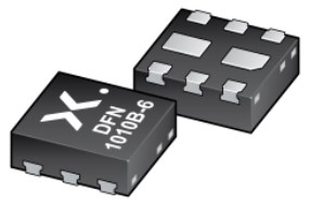
PMDXB950UPE is a dual P-channel enhancement mode Field-Effect Transistor. This article is going to talk about the features, applications, and more detailed information about PMDXB950UPE.

PMDXB950UPE is a dual P-channel enhancement mode Field-Effect Transistor. This article is going to talk about the features, applications, and more detailed information about PMDXB950UPE.
162
Apr 22, 2022
Sam Thomson
PMDXB950UPE is a dual P-channel enhancement mode Field-Effect Transistor. This article is going to talk about the features, applications, and more detailed information about PMDXB950UPE.
PMDXB950UPE
PMDXB950UPE Dual P-channel enhancement mode Field-Effect Transistor (FET) in a leadless ultra small DFN1010B-6 (SOT1216) Surface-Mounted Device (SMD) plastic package using Trench MOSFET technology.
Trench MOSFET technology
Leadless ultra-small and ultra-thin SMD plastic package: 1.1 × 1.0 × 0.37 mm
Exposed drain pad for excellent thermal conduction
ElectroStatic Discharge (ESD) protection > 1 kV HBM
Drain-source on-state resistance RDSon = 1.02 Ω
| Type Designator: PMDXB950UPE |
| Type of Transistor: MOSFET |
| Type of Control Channel: P -Channel |
| Maximum Power Dissipation (Pd): 0.265 W |
| Maximum Drain-Source Voltage |Vds|: 20 V |
| Maximum Gate-Source Voltage |Vgs|: 8 V |
| Maximum Gate-Threshold Voltage |Vgs(th)|: 0.95 V |
| Maximum Drain Current |Id|: 0.5 A |
| Maximum Junction Temperature (Tj): 150 °C |
| Total Gate Charge (Qg): 1.19 NC |
| Rise Time (tr): 5 nS |
| Drain-Source Capacitance (Cd): 14 pF |
| Maximum Drain-Source On-State Resistance (Rds): 1.4 Ohm |
| Package: DFN1010B-6 |
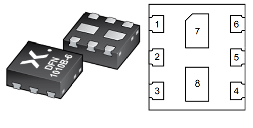
PMDXB950UPE Pinout

PMDXB950UPE Symbol

PMDXB950UPE Footprint
Nexperia PMDXB950UPE technical specifications, attributes, parameters and parts with similar specifications to Nexperia PMDXB950UPE.
Nexperia PMDXB950UPE technical specifications, attributes, parameters and parts with similar specifications to Nexperia PMDXB950UPE.
| Product Attribute | Attribute Value | |
|---|---|---|
| JESD-609 Code | e3 | |
| Moisture Sensitivity Level (MSL) | 1 (Unlimited) |
| Product Attribute | Attribute Value | |
|---|---|---|
| Terminal Finish | Tin (Sn) | |
| Reach Compliance Code | compliant |
| Product Attribute | Attribute Value | |
|---|---|---|
| RoHS Status | RoHS Compliant |
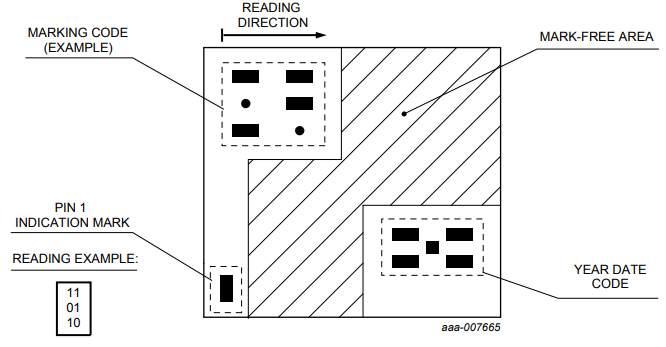
PMDXB950UPE Marking
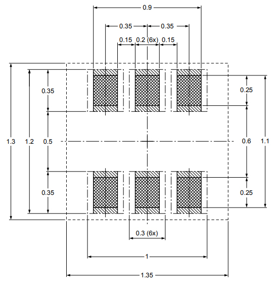
PMDXB950UPE Soldering
Relay driver
High-speed line driver
High-side load switch
Switching circuits
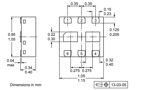
PMDXB950UPE Package information
Nexperia is a focused global leader in the fields of discretes, logic, and MOSFETs. At the start of 2017, this new company became self-sufficient. Nexperia focuses on efficiency and manufactures a high amount of dependably dependable semiconductor components: 85 billion per year. The company's comprehensive portfolio fulfills the Automotive industry's strict standards. And their industry-leading compact packages, which are built in-house, combine power and thermal efficiency with best-in-class quality. Nexperia has 11,000 personnel spread across Asia, Europe, and the United States, supporting customers all over the world.
TAGS
Comments