ATTENTION: Due to increased demand and order volume, processing time may take an additional 1-3 business days.
HomeCommunitySubjectSi3865BDV Load Switch with Level-Shift: Datasheet, Pinout, Application

Si3865BDV Load Switch with Level-Shift: Datasheet, Pinout, Application

PMIC - Power Distribution Switches, Load Drivers SOT-23-6 Thin, TSOT-23-6 General Purpose -55°C~150°C TJ Slew Rate Controlled SI3865 2.5V 175mOhm IC LOAD SWITCH LVL SHIFT 6-TSOP

86

Dec 4, 2021

Xenia Lynch

PMIC - Power Distribution Switches, Load Drivers SOT-23-6 Thin, TSOT-23-6 General Purpose -55°C~150°C TJ Slew Rate Controlled SI3865 2.5V 175mOhm IC LOAD SWITCH LVL SHIFT 6-TSOP

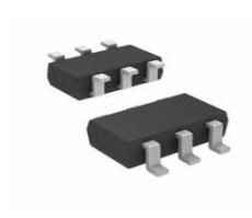
The Si3865BDV includes a p- and n-channel MOSFET in a single TSOP-6 package. This article will unlock more details about Si3865, including its datasheet, pinout, application and so on. Welcome your RFQ!
SI3865BDV-T1-E3

Inquiry
Min.: 1 Mult.: 1
Price not displayed? Not available to buy online? Please send an RFQ, and we will respond immediately.
Quick Links

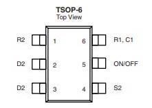
Si3865BDV Pinout

Si3865BDV CAD Model

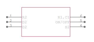
Si3865BDV Symbol


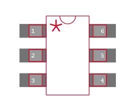
Si3865BDV Footprint


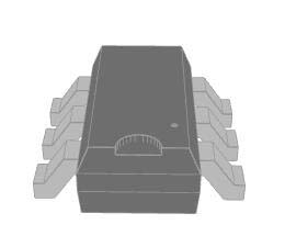
SI3865 3D Model

Si3865BDV Description

The Si3865BDV includes a p- and n-channel MOSFET in a single TSOP-6 package. The low on-resistance p-channel TrenchFET® is tailored for use as a load switch. The n-channel, with an external resistor, can be used as a level shift to drive the p-channel load-switch. The n-channel MOSFET has internal ESD protection and can be driven by logic signals as low as 1.5 V. The Si3865BDV operates on supply lines from 1.8 V to 8 V and can drive loads up to 2.9 A.

The Si3865BDV is ideally suited for high-side load switching in portable applications. The integrated N-Channel level-shift device saves space by reducing external components. The slew rate is set externally so that rise times can be tailored to different load types.

Si3865BDV Feature

  •  Halogen-free According to  IEC  61249-2-21 Definition

  • 60 mW Low RDS(on) TrenchFET®: 1.8 V Rated

  • 1.8 V to 8 V Input

  • 1.5 V to 8 V Logic Level Control

  • Low Profile, Small Footprint TSOP-6 Package

  • 3000 V ESD Protection On Input Switch, VON/OFF

  • Adjustable Slew-Rate

  • Compliant to  RoHS Directive  2002/95/EC

Si3865BDV Application

  • Ideally suited for high-side load switching in portable applications

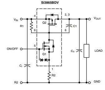
Si3865BDV Application Circuit

The following figures show the Si3865BDV application circuit:

Si3865BDV Application Circuit

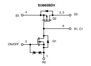
Si3865BDV Functional Block Diagram

The Si3865BDV Functional Block Diagram is given below:

SI3865BDV Functional Block Diagram

Specifications

Vishay Siliconix SI3865BDV-T1-E3 technical specifications, attributes, parameters and parts with similar specifications to Vishay Siliconix SI3865BDV-T1-E3.

SI3865BDV-T1-E3 Tech Specifications

Vishay Siliconix SI3865BDV-T1-E3 technical specifications, attributes, parameters and parts with similar specifications to Vishay Siliconix SI3865BDV-T1-E3.

Product Attribute Attribute Value
MountSurface Mount
Mounting TypeSurface Mount
Package / CaseSOT-23-6 Thin, TSOT-23-6
Number of Pins6Pins
Number of Elements2 Elements
Operating Temperature-55°C~150°C TJ
PackagingTape & Reel (TR)
Published2008
JESD-609 Codee3
Pbfree Codeyes
Part StatusObsolete
Moisture Sensitivity Level (MSL)1 (Unlimited)
Number of Terminations6Terminations
ECCN CodeEAR99
Resistance175mOhm
Terminal FinishMatte Tin (Sn)
Max Power Dissipation830mW
Terminal FormGULL WING
Product Attribute Attribute Value
Peak Reflow Temperature (Cel)260
Number of Functions1Function
Supply Voltage2.5V
Terminal Pitch0.95mm
Current Rating2.9A
Time@Peak Reflow Temperature-Max (s)40
Base Part NumberSI3865
Pin Count6
Number of Outputs1Output
Output TypeP-Channel
Supply Voltage-Max (Vsup)8V
InterfaceOn/Off
Element ConfigurationDual
Output ConfigurationHigh Side
Power Dissipation830mW
Output Current2.9A
Switch TypeGeneral Purpose
Drain to Source Voltage (Vdss)8V
Product Attribute Attribute Value
Continuous Drain Current (ID)2.9A
Ratio - Input:Output1:1
Voltage - Load1.8V~8V
Driver Number of Bits1Bit
Drain to Source Breakdown Voltage8V
Output Peak Current Limit-Nom1A
Rds On (Typ)45m Ω
Drain to Source Resistance60mOhm
Built-in ProtectionsTRANSIENT
FeaturesSlew Rate Controlled
Height990.6μm
Length3.0988mm
Width1.7018mm
REACH SVHCUnknown
Radiation HardeningNo
RoHS StatusROHS3 Compliant
Lead FreeLead Free
0 Products View Similar

Si3865BDV Manufacturer

Vishay's product portfolio is an unmatched collection of discrete semiconductors (diodes, MOSFETs, and optoelectronics) and passive components (resistors, inductors, and capacitors). These components are used in virtually all types of electronic devices and equipment in the industrial, computing, automotive, consumer, telecommunications, military, aerospace, and medical markets.  Vishay is proud to be a major partner with  Digi-Key.

Datasheet PDF

SI3865BDV-T1-E3 Documents

Download datasheets and manufacturer documentation for SI3865BDV-T1-E3

Datasheets
SI3865BDV
PCN Obsolescence/ EOL
PCN- SIL-0582013 05/Dec/2013

Frequently Asked Questions

What package does the Si3865BDV include a p- and n-channel MOSFET?
A single TSOP-6 package.
What is the low on-resistance p-channel designed for use as a load switch?
TrenchFET®.
What can be used as a level shift to drive the p-channel load-switch?
N-channel.
What is the Si3865BDV ideally suited for in portable applications?
High-side load switching.
What saves space by reducing external components?
N-Channel level-shift device.
FAQ
What package does the Si3865BDV include a p- and n-channel MOSFET?
A single TSOP-6 package.
What is the low on-resistance p-channel designed for use as a load switch?
TrenchFET®.
What can be used as a level shift to drive the p-channel load-switch?
N-channel.
What is the Si3865BDV ideally suited for in portable applications?
High-side load switching.
What saves space by reducing external components?
N-Channel level-shift device.

TAGS

Share