ATTENTION: Due to increased demand and order volume, processing time may take an additional 1-3 business days.
HomeCommunitySubjectSN65HVD230DR CAN Transceiver: Datasheet, Pinout, Schematic

SN65HVD230DR CAN Transceiver: Datasheet, Pinout, Schematic

TEXAS INSTRUMENTS - SN65HVD230DR - IC, CAN TRANSCEIVER, 1MBPS, 8SOIC

699

Aug 28, 2021

Dunn Stevenson

SN65HVD230 CAN bus transceiver


TEXAS INSTRUMENTS - SN65HVD230DR - IC, CAN TRANSCEIVER, 1MBPS, 8SOIC

The SN65HVD230 controller area network (CAN) transceivers are designed for use with the Texas Instruments TMS320Lx240x™; 3.3-V DSPs with CAN controllers, or with equivalent devices. This article will unlock more details about SN65HVD230DR.
SN65HVD230DR

50000In Stock
Min.: 1 Mult.: 1
Quantity Unit Price Ext. Price
1+ $1.99945$2
10+ $1.88627$18.86
100+ $1.7795$177.95
500+ $1.67878$839.39
1000+ $1.58375$1583.75
Unit Price:$1.99945
Subtotal: $2
Looking for a better price? Want a lower wholesale price? Please send an RFQ, and we will respond immediately.
Quick Links

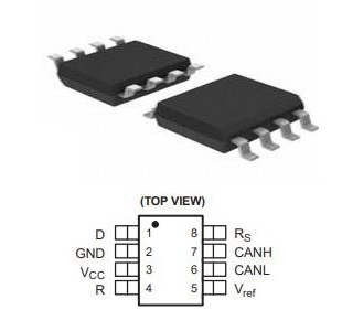
SN65HVD230DR Pinout

SN65HVD230DR CAD Model

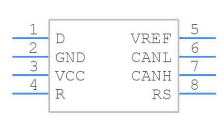
Symbol


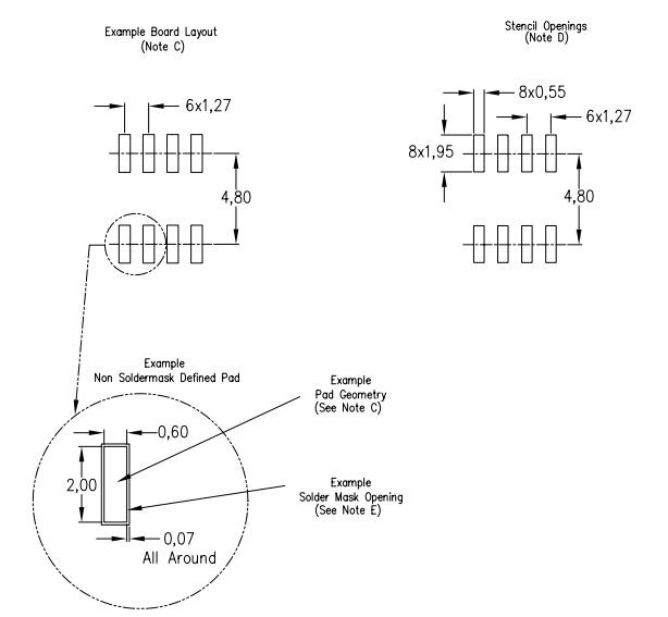
Footprint


3D Model


SN65HVD230DR Description

The SN65HVD230 controller area network (CAN) transceiver is designed for use with the Texas Instruments TMS320Lx240x™; 3.3-V DSPs with CAN controllers, or with equivalent devices. It is intended for use in applications employing the CAN serial communication physical layer in accordance with the ISO 11898 standard. Each CAN transceiver is designed to provide differential transmit capability to the bus and differential receive capability to a CAN controller at speeds up to 1 Mbps.

Specifications

Texas Instruments SN65HVD230DR technical specifications, attributes, parameters and parts with similar specifications to Texas Instruments SN65HVD230DR.

SN65HVD230DR Tech Specifications

Texas Instruments SN65HVD230DR technical specifications, attributes, parameters and parts with similar specifications to Texas Instruments SN65HVD230DR.

Product Attribute Attribute Value
Lifecycle StatusACTIVE (Last Updated: 2 days ago)
Factory Lead Time6 Weeks
Contact PlatingGold
Mounting TypeSurface Mount
Package / Case8-SOIC (0.154, 3.90mm Width)
Surface MountYES
Number of Pins8Pins
Weight72.603129mg
Number of I/Os2I/Os
Operating Temperature-40°C~85°C
PackagingCut Tape (CT)
JESD-609 Codee4
Pbfree Codeyes
Part StatusActive
Moisture Sensitivity Level (MSL)1 (Unlimited)
Product Attribute Attribute Value
Number of Terminations8Terminations
TerminationSMD/SMT
ECCN CodeEAR99
TypeTransceiver
Voltage - Supply3V~3.6V
Terminal PositionDUAL
Terminal FormGULL WING
Peak Reflow Temperature (Cel)260
Number of Functions1Function
Supply Voltage3.3V
Base Part Number65HVD230
Pin Count8
Operating Supply Voltage3.3V
Nominal Supply Current17mA
Max Supply Current17mA
Product Attribute Attribute Value
Slew Rate15 V/μs
Data Rate1Mbps
ProtocolCANbus
Number of Drivers/Receivers1/1Drivers/Receiver
DuplexHalf
Receiver Hysteresis100mV
Number of Receivers1Receiver
Height1.75mm
Length4.9mm
Width3.91mm
Thickness1.58mm
REACH SVHCNo SVHC
Radiation HardeningNo
RoHS StatusROHS3 Compliant
Lead FreeLead Free
0 Products View Similar

SN65HVD230DR Features

  • Operates With a 3.3-V Supply

  • Low Power Replacement for the PCA82C250 Footprint

  • Bus/Pin ESD Protection Exceeds 16 kV HBM

  • High Input Impedance Allows for 120 Nodes on a Bus

  • Controlled Driver Output Transition Times for

  • improved Signal Quality on the SN65HVD230 and SN65HVD231

  • Unpowered Node Does Not Disturb the Bus

  • Compatible With the Requirements of the Iso 11898 Standard

  • Low-Current SN65HVD230 Standby Mode 370 uA Tvoical

  • Designed for Signaling Rates(1) up to 1

  • Megabit/Second (Mbps)

  • Thermal Shutdown Protection

  • Open-Circuit Fail-Safe Design

  • Glitch-Free Power-Up and Power-Down

  • Protection for Hot-Plugging Applications

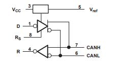
SN65HVD230DR Logic Diagram

SN65HVD230DR Application

  • Motor Control

  • Industrial Automation

  • Basestation Control and Status

  • Robotics

  • Automotive

  • UPS Control

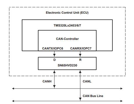
SN65HVD230DR Typical Application Schematic

The schematic below illustrates a typical application of the SN65HVD230 family. The output of a DSP's CAN controller is connected to the serial driver input, pin D, and receiver serial output, pin R, of the transceiver. The transceiver is then attached to the differential bus lines at pins CANH and CANL.

Details of a Typical CAN Node


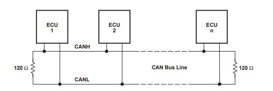
Typically, the bus is a twisted pair of wires with a characteristic impedance of 120 Ω, in the standard half-duplex multipoint topology of Typical CAN Network Schematic below. Each end of the bus is terminated with 120-Ω resistors in compliance with the standard to minimize signal reflections on the bus.

Typical CAN Network

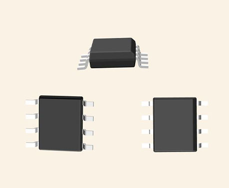
SN65HVD230DR Package

SN65HVD230DR Manufacturer

Texas Instruments (TI) is a global semiconductor firm originating in 1958 and nowadays it has over 30,000 employees who design, conduct and sell analogue and product-differentiating embedded processing components in 35 countries. Aimed at changing the world of tech, TI has put great effort into becoming the solution provider coupled with a vision.


Frequently Asked Questions

What is the SN65HVD230 designed for?
It is designed for operation in especially harsh environments, these devices feature cross-wire protection, loss-of-ground and overvoltage protection, over-temperature protection, as well a wide common-mode range.
What differences is between the SN65HVD230 and SN65HVD231?
On the SN65HVD230 and SN65HVD231, pin 8 provides three different modes of operation: high-speed, slope control, and low-power modes. The high-speed mode of operation is selected by connecting pin 8 to the ground, allowing the transmitter output transistors to switch on and off as fast as possible with no limitation on the rise and fall slopes. The rise and fall slopes can be adjusted by connecting a resistor to the ground at pin 8 since the slope is proportional to the pin's output current. This slope control is implemented with external resistor values of 10 kΩ, to achieve a 15-V/μs slew rate, to 100 kΩ, to achieve a 2-V/μs slew rate. See the Application Information section of this datasheet. The unique difference between the SN65HVD230 and the SN65HVD231 is that both the driver and the receiver are switched off in the SN65HVD231 when a high logic level is applied to pin 8 and remain in this sleep mode until the circuit is reactivated by a low logic level on pin 8. The Vref pin 5 on the SN65HVD230 and SN65HVD231 is available as a VCC/2 voltage reference.
FAQ
What is the SN65HVD230 designed for?
It is designed for operation in especially harsh environments, these devices feature cross-wire protection, loss-of-ground and overvoltage protection, over-temperature protection, as well a wide common-mode range.
What differences is between the SN65HVD230 and SN65HVD231?
On the SN65HVD230 and SN65HVD231, pin 8 provides three different modes of operation: high-speed, slope control, and low-power modes. The high-speed mode of operation is selected by connecting pin 8 to the ground, allowing the transmitter output transistors to switch on and off as fast as possible with no limitation on the rise and fall slopes. The rise and fall slopes can be adjusted by connecting a resistor to the ground at pin 8 since the slope is proportional to the pin's output current. This slope control is implemented with external resistor values of 10 kΩ, to achieve a 15-V/μs slew rate, to 100 kΩ, to achieve a 2-V/μs slew rate. See the Application Information section of this datasheet. The unique difference between the SN65HVD230 and the SN65HVD231 is that both the driver and the receiver are switched off in the SN65HVD231 when a high logic level is applied to pin 8 and remain in this sleep mode until the circuit is reactivated by a low logic level on pin 8. The Vref pin 5 on the SN65HVD230 and SN65HVD231 is available as a VCC/2 voltage reference.

TAGS

Share