ATTENTION: Due to increased demand and order volume, processing time may take an additional 1-3 business days.
HomeCommunitySubjectSN74AXC8T245RJWR Bus Transceiver: Schematic, Pinout, and Datasheet

SN74AXC8T245RJWR Bus Transceiver: Schematic, Pinout, and Datasheet

24 PIN TRANSLATOR ISL2 COBRA The SN74AXC8T245RJWR is an 8-Bit Dual-Supply Bus Transceiver With Configurable Voltage Translation and Tri-State Outputs.

187

Apr 1, 2022

Alan Eleanor

Bus Transceiver


24 PIN TRANSLATOR ISL2 COBRA

The SN74AXC8T245RJWR is an 8-Bit Dual-Supply Bus Transceiver With Configurable Voltage Translation and Tri-State Outputs. This article mainly introduces Schematic, Pinout, Datasheet and other detailed information about Texas Instruments SN74AXC8T245RJWR.


SN74AXC8T245RJWR

48123In Stock
Min.: 1 Mult.: 1
Quantity Unit Price Ext. Price
1+ $2.01481$2.01
10+ $1.90077$19.01
100+ $1.79318$179.32
500+ $1.69168$845.84
1000+ $1.59592$1595.92
Unit Price:$2.01481
Subtotal: $2.01
Looking for a better price? Want a lower wholesale price? Please send an RFQ, and we will respond immediately.
Quick Links

SN74AXC8T245RJWR Description

The SN74AXC8T245RJWR is an 8-bit non-inverting bus transceiver that corrects voltage level mismatches between devices running at the most recent voltage nodes (0.7 V, 0.8 V, and 0.9 V) and devices operating at industry standard voltage nodes (1.8 V, 2.5 V, 3.3 V) and vice versa.

Two independent power supply rails (VCCA and VCCB) run at as low as 0.65 V to power the gadget. A1 through A8 are data pins that track VCCA, which accepts any source voltage between 0.65 and 3.6 V. VCCB, which accepts any supply voltage between 0.65 V and 3.6 V, is tracked by data pins B1 through B8.

The SN74AXC8T245RJWR device is intended for asynchronous data bus connections. Depending on the logic level of the direction-control inputs (DIR1 and DIR2), the device transfers data from the A bus to the B bus or from the B bus to the A bus. The output-enable (OE) input is used to disable the outputs, thus isolating the buses.

The control pins (DIR and OE) of the SN74AXC8T245RJWR device are referred to VCCA.

This device is completely qualified for Ioff-based partial-power-down applications. When the device is turned off, the Ioff circuitry shuts the outputs. This prevents current backflow into the device, preventing device damage.

If each VCC input supply falls below 100 mV, the VCC isolation function disables all level shifter outputs and places them in a high-impedance condition.

OE should be coupled to VCCA through a pullup resistor to assure the high-impedance condition of the level shifter  I/Os during power up or power down; the minimum value of the resistor is decided by the driver's current-sinking capabilities.


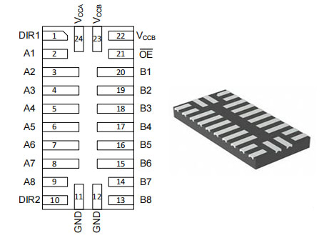
SN74AXC8T245RJWR Pinout

Pinout


Pin Number Pin Name Description
2 A1 Input/output A1. Referenced to VCCA
3 A2 Input/output A2. Referenced to VCCA
4 A3 Input/output A3. Referenced to VCCA
5 A4 Input/output A4. Referenced to VCCA
6 A5 Input/output A5. Referenced to VCCA
7 A6 Input/output A6. Referenced to VCCA
8 A7 Input/output A7. Referenced to VCCA
9 A8 Input/output A8. Referenced to VCCA
20 B1 Input/output B1. Referenced to VCCB.
19 B2 Input/output B2. Referenced to VCCB.
18 B3 Input/output B3. Referenced to VCCB.
17 B4 Input/output B4. Referenced to VCCB.
16 B5 Input/output B5. Referenced to VCCB.
15 B6 Input/output B6. Referenced to VCCB.
14 B7 Input/output B7. Referenced to VCCB.
13 B8 Input/output B8. Referenced to VCCB.
1 DIR1 Direction-control signal. Referenced to VCCA.
10 DIR2 Direction-control signal when both VCCA and VCCB ≥ 1.4 V.
Referenced to VCCA. Tie to GND to maintain backward compatibility with SN74AVC8T245 device.
11,12 GND Ground
21 OE Output Enable. Pull to GND to enable all outputs. Pull to VCCA to place all outputs in high-impedance mode. Referenced to VCCA.
24 VCCA A-port supply voltage. 0.65 V ≤ VCCA ≤ 3.6 V
22,23 VCCB B-port supply voltage. 0.65 V ≤ VCCB ≤ 3.6 V

SN74AXC8T245RJWR CAD Model

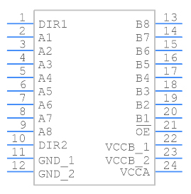
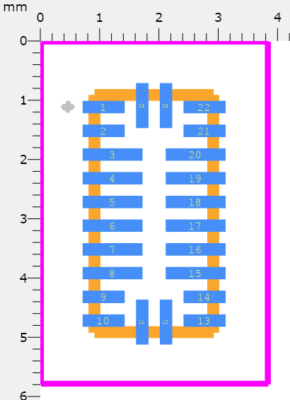
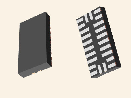
The following show SN74AXC8T245RJWR Symbol, Footprint and 3D Model.

Symbol

Footprint

3D Model

SN74AXC8T245RJWR Features

• Qualified Fully Configurable Dual-Rail Design Allows Each Port to Operate With a Power Supply Range From 0.65 V to 3.6 V

• Operating Temperature From –40°C to +125°C

• Multiple Direction Control Pins to Allow Simultaneous Up and Down Translation

• Up to 380 Mbps Support When Translating from 1.8 V to 3.3 V

• VCC Isolation Feature to Effectively Isolate Both Buses in a Power-Down Scenario

• Partial Power-Down Mode to Limit Backflow Current in a Power-Down Scenario

• Compatible With SN74AVC8T245 and 74AVC8T245 Level Shifters

• Latch-Up Performance Exceeds 100 mA Per JESD 78, Class II

• ESD Protection Exceeds JESD 22

– 8000-V  Human-Body Model 

– 1000-V Charged-Device Model

Specifications

SN74AXC8T245RJWR Tech Specifications

Texas Instruments SN74AXC8T245RJWR technical specifications, attributes, parameters and parts with similar specifications to Texas Instruments SN74AXC8T245RJWR.

Product Attribute Attribute Value
Factory Lead Time6 Weeks
Mounting TypeSurface Mount
Package / Case24-UFQFN
Surface MountYES
Operating Temperature-40°C~125°C TA
PackagingTape & Reel (TR)
Series74AXC
Pbfree Codeyes
Part StatusActive
Moisture Sensitivity Level (MSL)1 (Unlimited)
Number of Terminations24Terminations
Product Attribute Attribute Value
Terminal PositionQUAD
Terminal FormNO LEAD
Number of Functions1Function
Supply Voltage0.7V
Terminal Pitch0.4mm
Base Part Number74AXC8T245
JESD-30 CodeR-PQCC-N24
Output Type3-State
Supply Voltage-Max (Vsup)3.6V
Supply Voltage-Min (Vsup)0.65V
Number of Ports2Ports
Product Attribute Attribute Value
Number of Bits8Bits
FamilyAXC
Output PolarityTRUE
Logic IC TypeBUS TRANSCEIVER
Max I(ol)0.012 A
Propagation Delay (tpd)172 ns
Power Supply Current-Max (ICC)0.055mA
Length4mm
Height Seated (Max)0.55mm
Width2mm
RoHS StatusROHS3 Compliant
0 Products View Similar

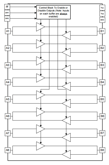
SN74AXC8T245RJWR Functional Block Diagram

The following figure is SN74AXC8T245RJWR Functional Block Diagram.

Functional Block Diagram

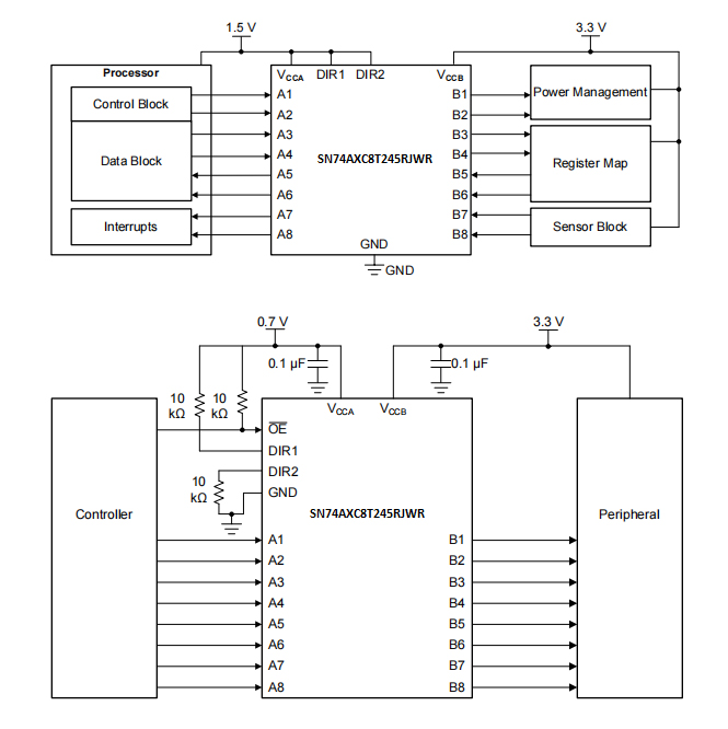
SN74AXC8T245RJWR Typical Application Schematic

The SN74AXC8T245RJWR Typical Application Schematics are shown as follows.

Typical Application Schematic

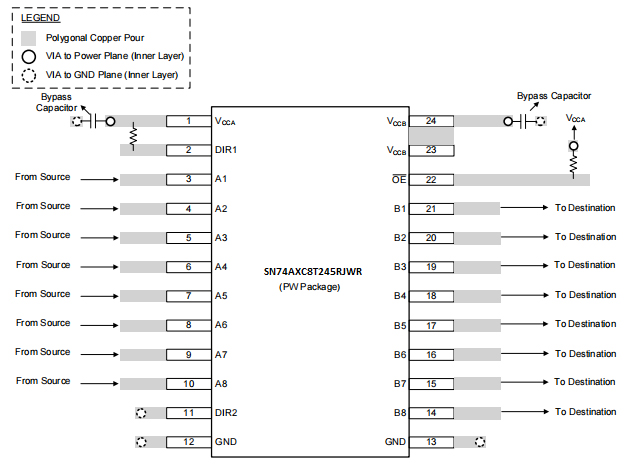
SN74AXC8T245RJWR Layout

Follow standard printed-circuit board layout principles to ensure device reliability.

• On power supplies, use bypass capacitors.

• To avoid excessive loading, use short trace lengths.

• Depending on the system needs, place pads on the signal channels for loading capacitors or pullup resistors to help regulate the signal rise and fall times.

Layout

SN74AXC8T245RJWR Alternatives

Part Number Description Manufacturer
SN74AVCH245DGVRLOGIC AVC SERIES, 8-BIT TRANSCEIVER, TRUE OUTPUT, PDSO20, PLASTIC, TVSOP-20 Texas Instruments
SN74AVC245DGVRLOGIC AVC SERIES, 8-BIT TRANSCEIVER, TRUE OUTPUT, PDSO20, PLASTIC, TVSOP-20 Texas Instruments
SN74AVCH244DWRLOGIC IC AVC SERIES, DUAL 4-BIT DRIVER, TRUE OUTPUT, PDSO20, PLASTIC, SO-20, Bus Driver/Transceiver Texas Instruments
SN74AVCH245DGVLOGIC AVC SERIES, 8-BIT TRANSCEIVER, TRUE OUTPUT, PDSO20, PLASTIC, TVSOP-20 Texas Instruments
SN74AVC245DWRLOGIC AVC SERIES, 8-BIT TRANSCEIVER, TRUE OUTPUT, PDSO20, PLASTIC, SOP-20 Texas Instruments
SN74AVC32T245GKERLOGIC 32-Bit Dual-Supply Bus Transceiver with Configurable Voltage Translation and 3-State Outputs 96-LFBGA -40 to 85 Texas Instruments
SN74AVCH244DGVRLOGIC AVC SERIES, DUAL 4-BIT DRIVER, TRUE OUTPUT, PDSO20, TVSOP-20 Texas Instruments
SN74AVC245DGVLOGIC AVC SERIES, 8-BIT TRANSCEIVER, TRUE OUTPUT, PDSO20, PLASTIC, TVSOP-20 Texas Instruments
SN74AVC244DWLOGIC IC AVC SERIES, DUAL 4-BIT DRIVER, TRUE OUTPUT, PDSO20, PLASTIC, SO-20, Bus Driver/Transceiver Texas Instruments
SN74AVC32T245ZRLRLOGIC 32-Bit Dual-Supply Bus Transceiver with Configurable Voltage Translation and 3-State Outputs 96-BGA MICROSTAR JUNIOR -40 to 85 Texas Instruments

SN74AXC8T245RJWR Applications

• Enterprise and Communications

• Industrial

• Personal Electronics

• Wireless Infrastructure

• Building Automation

• Point of Sale

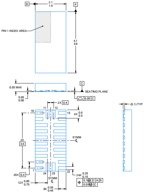
SN74AXC8T245RJWR Package

The following figure is SN74AXC8T245RJWR Package.

Package

SN74AXC8T245RJWR Manufacturer

Texas Instruments Incorporated (TI) is an American technology corporation based in Dallas, Texas, that creates and manufactures semiconductors and integrated circuits for sale to electronics designers and manufacturers across the world. Based on sales volume, it is among the top ten semiconductor businesses in the world. More than 80% of the company's income comes from analog chips and embedded CPUs. In addition to calculators, microcontrollers, and multi-core computers, TI manufactures TI digital light processing technologies and education technology.

Frequently Asked Questions

What is a bus transceiver?
Bus transceivers are tri-state bi-directional devices that allow the flow of data between two points making them compatible with bus-oriented systems or the bi-directional (input or output) control of interface circuitry. Bus transceivers can be inverting, the TTL 74LS242, or non-inverting, the TTL 74LS243 devices.
How does bus transceiver work?
The role of the transceiver is simply to drive and detect data to and from the bus. It converts the single-ended logic used by the controller to the differential signal transmitted over the bus. The transceiver distinguishes between two bus logic states, dominant and recessive.
How low do two independent power supply rails run to power the gadget?
0.65 V.
What is the SN74AXC8T245RJWR device intended for?
Asynchronous data bus connections.
What is the logic level of the SN74AXC8T245RJWR device?
Direction-control inputs.
What is used to disable the outputs of the SN74AXC8T245RJWR?
Output-enable.
What is the name of the control pins used by the SN74AXC8T245RJWR device?
VCCA.
What type of applications are the control pins of the SN74AXC8T245RJWR referred to as?
Partial-power-down.
What does the Ioff circuitry do when the device is turned off?
Shuts the outputs.
What happens when the Ioff circuitry shuts the outputs of the SN74AXC8T245RJWR?
Current backflow into the device.
What is used to ensure the high-impedance condition of the level shifter I/Os during power up or power down?
A pullup resistor.
FAQ
What is a bus transceiver?
Bus transceivers are tri-state bi-directional devices that allow the flow of data between two points making them compatible with bus-oriented systems or the bi-directional (input or output) control of interface circuitry. Bus transceivers can be inverting, the TTL 74LS242, or non-inverting, the TTL 74LS243 devices.
How does bus transceiver work?
The role of the transceiver is simply to drive and detect data to and from the bus. It converts the single-ended logic used by the controller to the differential signal transmitted over the bus. The transceiver distinguishes between two bus logic states, dominant and recessive.
How low do two independent power supply rails run to power the gadget?
0.65 V.
What is the SN74AXC8T245RJWR device intended for?
Asynchronous data bus connections.
What is the logic level of the SN74AXC8T245RJWR device?
Direction-control inputs.
What is used to disable the outputs of the SN74AXC8T245RJWR?
Output-enable.
What is the name of the control pins used by the SN74AXC8T245RJWR device?
VCCA.
What type of applications are the control pins of the SN74AXC8T245RJWR referred to as?
Partial-power-down.
What does the Ioff circuitry do when the device is turned off?
Shuts the outputs.
What happens when the Ioff circuitry shuts the outputs of the SN74AXC8T245RJWR?
Current backflow into the device.
What is used to ensure the high-impedance condition of the level shifter I/Os during power up or power down?
A pullup resistor.

TAGS

Share