ATTENTION: Due to increased demand and order volume, processing time may take an additional 1-3 business days.
HomeCommunitySubjectSN74LV1T125DCKR Single Buffer Gate: Package, Pinout, and Datasheet

SN74LV1T125DCKR Single Buffer Gate: Package, Pinout, and Datasheet

IC BUF NON-INVERT 5.5V SC70-5 For industrial, portable, telecom, and automotive applications, the SN74LV1T125DCKR is a low voltage CMOS gate logic that operates across a larger voltage range.

98

Apr 19, 2022

Rae Paul

Buffer Gate


IC BUF NON-INVERT 5.5V SC70-5

For industrial, portable, telecom, and automotive applications, the SN74LV1T125DCKR is a low voltage CMOS gate logic that operates across a larger voltage range. This article mainly introduces Package, Pinout, Datasheet and other detailed information about Texas Instruments SN74LV1T125DCKR.


SN74LV1T125DCKR

693In Stock
Min.: 1 Mult.: 1
Price not displayed? Not available to buy online? Please send an RFQ, and we will respond immediately.
Quick Links

SN74LV1T125DCKR Description

For industrial, portable, telecom, and automotive applications, the SN74LV1T125DCKR is a low voltage CMOS gate logic that operates across a larger voltage range. The output level is related to the supply voltage and can accommodate CMOS levels of 1.8V/2.5V/3.3V/5V.

The input is built with a lower threshold circuit to match 1.8V input logic at VCC = 3.3V and can be used in level up translation from 1.8V to 3.3V. Down translation (e.g. 3.3V to 2.5V output at VCC = 2.5V) is also possible thanks to the 5V tolerant input pins. The VCC range of 1.8V to 5.5V allows for the production of desired output levels for controllers or processors.

To prevent line reflections, overshoot, and undershoot produced by high-drive outputs, the SN74LV1T125DCKR is designed with a current-drive capability of 8 mA.

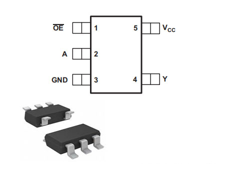
SN74LV1T125DCKR Pinout

Pinout


Pin Number Pin Name Description
1 OE OE Enable/Input
2 A Input
3 GND Ground
4 Y Output
5 VCC Power pin

SN74LV1T125DCKR CAD Model

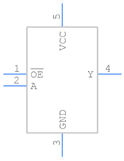
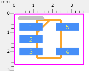
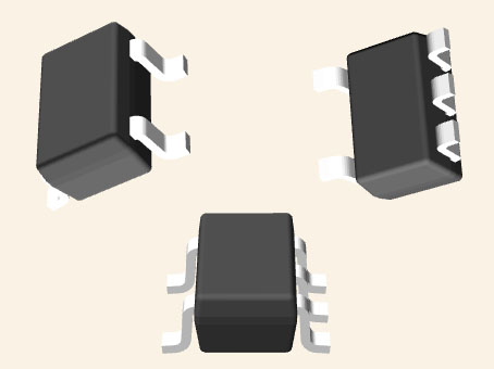
The following figures are SN74LV1T125DCKR Symbol, Footprint and 3D Model.

Symbol

Footprint

3D Model

SN74LV1T125DCKR Features

• Single-Supply Voltage Translator at 5.0/3.3/2.5/1.8V  VCC 

• Operating Range of 1.8V to 5.5V

• Up Translation

– 1.2V to 1.8V at 1.8V VCC

– 1.5V to 2.5V at 2.5V VCC

– 1.8V to 3.3V at 3.3V VCC

– 3.3V to 5.0V at 5.0VVCC

• Down Translation

– 3.3V to 1.8V at 1.8V VCC

– 3.3V to 2.5V at 2.5V VCC

– 5.0V to 3.3V at 3.3V VCC

• Logic Output is Referenced to VCC

• Output Drive

– 8.0mA Output Drive at 5.0V

– 7.0mA Output Drive at 3.3V

– 3.0mA Output Drive at 1.8V

• Characterized up to 50MHz at 3.3V VCC

• 5.0V Tolerance on Input Pins

• –40°C to 125°C Operating Temperature Range

•  Latch-Up  Performance Exceeds 250mA Per JESD 17

• ESD Performance Tested Per JESD 22

– 2000-V Human-Body Model (A114-B, Class II)

– 200-V Machine Model (A115-A)

– 1000-V  Charged-Device Model  (C101)

• Supports Standard Logic Pinouts

• CMOS Output B Compatible with AUP1G and LVC1G Families

Specifications

SN74LV1T125DCKR Tech Specifications

Texas Instruments SN74LV1T125DCKR technical specifications, attributes, parameters and parts with similar specifications to Texas Instruments SN74LV1T125DCKR.

Product Attribute Attribute Value
Lifecycle StatusACTIVE (Last Updated: 1 day ago)
Factory Lead Time6 Weeks
Contact PlatingGold
MountSurface Mount
Mounting TypeSurface Mount
Package / Case5-TSSOP, SC-70-5, SOT-353
Number of Pins5Pins
Weight6.095147mg
Operating Temperature-40°C~125°C TA
PackagingTape & Reel (TR)
Series74LV
JESD-609 Codee4
Pbfree Codeyes
Part StatusActive
Moisture Sensitivity Level (MSL)1 (Unlimited)
Number of Terminations5Terminations
ECCN CodeEAR99
Packing MethodTR
Product Attribute Attribute Value
Voltage - Supply1.6V~5.5V
Terminal PositionDUAL
Terminal FormGULL WING
Number of Functions1Function
Supply Voltage1.8V
Base Part Number74LV1T125
Output Type3-State
PolarityNon-Inverting
Power Supplies3.3V
Number of Channels1Channel
Operating Supply Current8mA
Load Capacitance30pF
Number of Ports2Ports
Nominal Supply Current8mA
Number of Bits1Bit
Propagation Delay16 ns
Quiescent Current1μA
FamilyLV/LV-A/LVX/H
Product Attribute Attribute Value
Logic FunctionInverting
Logic TypeBuffer, Non-Inverting
Max I(ol)0.008 A
Prop. Delay@Nom-Sup9 ns
Control TypeENABLE LOW
Number of Output Lines1Output Line
Count DirectionUNIDIRECTIONAL
Ambient Temperature Range High125°C
Height1.1mm
Length2mm
Width1.25mm
Thickness900μm
REACH SVHCNo SVHC
Radiation HardeningNo
RoHS StatusROHS3 Compliant
Lead FreeLead Free
0 Products View Similar

SN74LV1T125DCKR Typical Design Examples

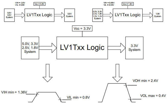
The following is SN74LV1T125DCKR Typical Design Examples.

Switching Thresholds for 1.8-V to 3.3-V Translation


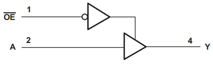
SN74LV1T125DCKR Logic Diagram

The following is SN74LV1T125DCKR Logic Diagram.

Logic Diagram

SN74LV1T125DCKR Alternatives

Part Number Description Manufacturer
74LVC1G125GW,115LOGIC 74LVC1G125 - Bus buffer/line driver; 3-state@en-us TSSOP 5-Pin Nexperia
74LVC1G125SE-7LOGIC Bus Driver, LVC/LCX/Z Series, 1-Func, 1-Bit, True Output, CMOS, PDSO5, ROHS COMPLIANT, SOT-353, 5 PIN Diodes Incorporated
74LVC1G125GWLOGIC Bus Driver, 1-Func, 1-Bit, True Output, CMOS, PDSO5, Philips Semiconductors
CLVC1G125IDCKREPLOGIC Enhanced product single 1.65-V to 5.5-V buffer with 3-state outputs 5-SC70 -40 to 85 Texas Instruments
935268720118LOGIC Bus Driver Nexperia
935268720125LOGIC Bus Driver, LVC/LCX/Z Series, 1-Func, 1-Bit, True Output, CMOS, PDSO5 Nexperia
74LVC1G125GW,118LOGIC 74LVC1G125 - Bus buffer/line driver; 3-state@en-us TSSOP 5-Pin Nexperia

SN74LV1T125DCKR Applications

• Industrial controllers

• Telecom

• Portable applications

• Servers

• PC and notebooks

• Automotive

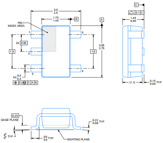
SN74LV1T125DCKR Package

The following figure is SN74LV1T125DCKR Package.

Package

SN74LV1T125DCKR Manufacturer

Texas Instruments Incorporated (TI) is an American technology corporation based in Dallas, Texas, that designs and manufactures semiconductors and different integrated circuits for electronic designers and manufacturers around the world. On the basis of sales volume, it is one of the top ten semiconductor businesses in the world. The company's main focus is on analog chips and embedded processors, which account for over 80% of its revenue. Calculators, microcontrollers, and multi-core processors are among the TI digital light processing technology and education technology products.

Datasheet PDF

SN74LV1T125DCKR Documents

Download datasheets and manufacturer documentation for SN74LV1T125DCKR

PCN Assembly/Origin
Mult Devices 02/Oct/2017

Frequently Asked Questions

What is single buffer gate?
The Single Buffer Gate is a low voltage CMOS gate logic that operates at a wider voltage range for industrial, portable, telecom, and automotive applications.
What is buffer gate?
The Buffer Gate is a logic block that takes any input and compares the value to 0. If the input signal is zero, the output will be zero. If the input is non-zero, the output will be a “1” in the bit position designated by the drop-down box.
How do buffer gates work?
A buffer is a basic logic gate that passes its input, unchanged, to its output. Its behavior is the opposite of a NOT gate. The main purpose of a buffer is to regenerate the input, usually using a strong high and a strong low.
What is the SN74LV1T125DCKR?
A low voltage CMOS gate logic.
What is the output level of the SN74LV1T125DCKR related to?
Supply voltage.
What is the output level of the SN74LV1T125DCKR?
1.8V input logic.
What is possible thanks to the 5V tolerant input pins?
Down translation.
What is the SN74LV1T125DCKR a low voltage CMOS gate logic?
5V tolerant input pins.
What VCC range allows for the production of desired output levels for controllers or processors?
1.8V to 5.5V.
What is the current-drive capability of the SN74LV1T125DCKR?
8 mA.
FAQ
What is single buffer gate?
The Single Buffer Gate is a low voltage CMOS gate logic that operates at a wider voltage range for industrial, portable, telecom, and automotive applications.
What is buffer gate?
The Buffer Gate is a logic block that takes any input and compares the value to 0. If the input signal is zero, the output will be zero. If the input is non-zero, the output will be a “1” in the bit position designated by the drop-down box.
How do buffer gates work?
A buffer is a basic logic gate that passes its input, unchanged, to its output. Its behavior is the opposite of a NOT gate. The main purpose of a buffer is to regenerate the input, usually using a strong high and a strong low.
What is the SN74LV1T125DCKR?
A low voltage CMOS gate logic.
What is the output level of the SN74LV1T125DCKR related to?
Supply voltage.
What is the output level of the SN74LV1T125DCKR?
1.8V input logic.
What is possible thanks to the 5V tolerant input pins?
Down translation.
What is the SN74LV1T125DCKR a low voltage CMOS gate logic?
5V tolerant input pins.
What VCC range allows for the production of desired output levels for controllers or processors?
1.8V to 5.5V.
What is the current-drive capability of the SN74LV1T125DCKR?
8 mA.

TAGS

Share