ATTENTION: Due to increased demand and order volume, processing time may take an additional 1-3 business days.
HomeCommunitySubjectSN74LVC1G06DCKR Single Inverter Buffer/Driver: Diagram, Pinout, and Datasheet

SN74LVC1G06DCKR Single Inverter Buffer/Driver: Diagram, Pinout, and Datasheet

IC BUFFER INVERT 5.5V SC70-5 The 1.65-V to 5.5-V VCC operation of the SN74LVC1G06DCKR single inverter buffer and driver is specified. This article mainly introduces Diagram, Pinout, Datasheet and other detailed information about Texas Instruments SN74LVC1G06DCKR.

161

Apr 13, 2022

Maurice Moll

Variable Frequency Driver | Variable Inverter


IC BUFFER INVERT 5.5V SC70-5

The 1.65-V to 5.5-V VCC operation of the SN74LVC1G06DCKR single inverter buffer and driver is specified. This article mainly introduces Diagram, Pinout, Datasheet and other detailed information about Texas Instruments SN74LVC1G06DCKR.

SN74LVC1G06DCKR

632In Stock
Min.: 1 Mult.: 1
Price not displayed? Not available to buy online? Please send an RFQ, and we will respond immediately.
Quick Links

SN74LVC1G06DCKR Description

The 1.65-V to 5.5-V VCC operation of the SN74LVC1G06DCKR single inverter buffer and driver is specified.

The use of the die as the package in NanoFree package technology is a significant advancement in IC packaging concepts.

The SN74LVC1G06DCKR device has an open-drain output that may be coupled to other open-drain outputs to create active-low wired-OR and active-high wired-AND functions.  Sink  current is limited to 32 mA.

This device is completely specified for Ioff applications that require partial power down.

When the device is shut down, the Ioff circuitry turns off the outputs. This stops current from flowing back into the gadget, preventing it from being damaged.

SN74LVC1G06DCKR Pinout

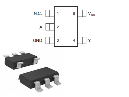
The following figure is SN74LVC1G06DCKR Pinout.

Pinout


Pin Number Pin Name Description
1 NC Not connected
2 A Input
3 GND Ground
4 Y Output
5 VCC Power pin

SN74LVC1G06DCKR CAD Model

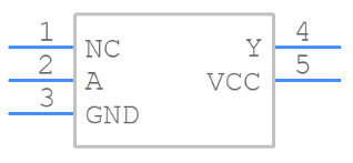
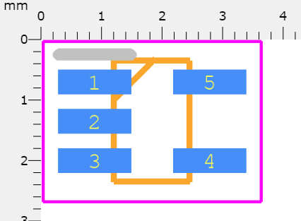
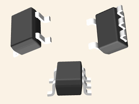
The following figures are SN74LVC1G06DCKR Symbol, Footprint and 3D Model.

Symbol

Footprint

3D Model

SN74LVC1G06DCKR Features

• ESD Protection Exceeds JESD 22

– 2000-V Human Body Model (A114-A)

– 200-V Machine Model (A115-A)

– 1000-V  Charged-Device Model  (C101)

• Available in the  Texas Instruments  NanoFree™ Package

• Supports 5-V VCC Operation

• Input and Open-Drain Output Accept Voltages up to 5.5 V

• Maximum tpd of 4.5 ns at 3.3 V at 125°C

• Low Power Consumption, 10-µA Maximum ICC

• ±24-mA Output Drive at 3.3 V for open-drain devices

• Ioff Supports Partial-Power-Down Mode and BackDrive Protection

•  Latch-Up  Performance Exceeds 100 mA Per JESD 78, Class II

• Can Be Used For Up or Down Translation

•  Schmitt Trigger  Action on All Ports

Specifications

SN74LVC1G06DCKR Tech Specifications

Texas Instruments SN74LVC1G06DCKR technical specifications, attributes, parameters and parts with similar specifications to Texas Instruments SN74LVC1G06DCKR.

Product Attribute Attribute Value
Lifecycle StatusACTIVE (Last Updated: 4 days ago)
Factory Lead Time6 Weeks
Contact PlatingGold
MountSurface Mount
Mounting TypeSurface Mount
Package / Case5-TSSOP, SC-70-5, SOT-353
Number of Pins5Pins
Operating Temperature-40°C~125°C
PackagingTape & Reel (TR)
Series74LVC
JESD-609 Codee4
Pbfree Codeyes
Part StatusActive
Moisture Sensitivity Level (MSL)1 (Unlimited)
Number of Terminations5Terminations
ECCN CodeEAR99
Product Attribute Attribute Value
Packing MethodTR
Voltage - Supply1.65V~5.5V
Terminal PositionDUAL
Terminal FormGULL WING
Peak Reflow Temperature (Cel)260
Number of Functions1Function
Supply Voltage1.8V
Base Part Number74LVC1G06
Pin Count5
Output TypeOpen Drain
PolarityInverting
Power Supplies3.3V
Number of Channels1Channel
Output Current32mA
Propagation Delay6.5 ns
Quiescent Current10μA
Product Attribute Attribute Value
Turn On Delay Time3 ns
FamilyLVC/LCX/Z
Logic FunctionBuffer, Inverter
Number of Inputs1Input
Logic TypeBuffer, Inverting
Max I(ol)0.032 A
Schmitt TriggerYES
Height1.1mm
Length2mm
Width1.25mm
Thickness900μm
REACH SVHCNo SVHC
Radiation HardeningNo
RoHS StatusROHS3 Compliant
Lead FreeLead Free
0 Products View Similar

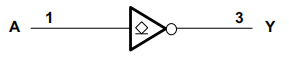
SN74LVC1G06DCKR Functional Block Diagram

The following figure is SN74LVC1G06DCKR Functional Block Diagram.

Functional Block Diagram

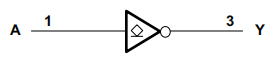
SN74LVC1G06DCKR Logic Diagram

The SN74LVC1G06DCKR Logic Diagram is shown as follows.

Positive Logic

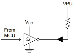
SN74LVC1G06DCKR Typical Application

The SN74LVC1G06DCKR Typical Application is shown as follows.

Typical Application

SN74LVC1G06DCKR Layout

Inputs must never float when using multiple-bit logic devices. When only two inputs of a triple-input AND gate are used, or only three of the four buffer gates are used, functionalities or parts of functions of digital logic devices are frequently left unused. The undefined voltages at the outside connections result in undefined operating states, hence such input pins must not be left disconnected. The rules that must be followed in all instances are listed below. To prevent floating, all unused inputs of digital logic devices must be connected to a high or low bias. The logic level that should be applied to any given unused input is determined by the device's function. They'll usually be connected to GND or VCC, depending on which makes more sense or is handier.

Layout

SN74LVC1G06DCKR Alternatives

Part Number Description Manufacturer
SN74LVC1G06DCKTE4LOGIC Single 1.65-V to 5.5-V inverter with open-drain outputs 5-SC70 -40 to 125 Texas Instruments
SN74LVC1G06DCKTLOGIC LVC/LCX/Z SERIES, 1-INPUT INVERT GATE, PDSO5, GREEN, PLASTIC, SC-70, 5 PIN Rochester Electronics LLC
SN74LVC1G06DCKLOGIC LVC/LCX/Z SERIES, 1-INPUT INVERT GATE, PDSO5, PLASTIC, SOT-5 Texas Instruments
SN74LVC1G06DCKRE4LOGIC Single 1.65-V to 5.5-V inverter with open-drain outputs 5-SC70 -40 to 125 Texas Instruments
SN74LVC1G06DCKRG4LOGIC Single 1.65-V to 5.5-V inverter with open-drain outputs 5-SC70 -40 to 125 Texas Instruments

SN74LVC1G06DCKR Applications

• AV Receivers

• Blu-ray Players and Home Theaters

• DVD Recorders and Players

• Desktop or Notebook PCs

• Digital Radio or Internet Radio Players

• Digital Video Cameras (DVC)

• Embedded PCs

• GPS: Personal Navigation Devices

• Mobile Internet Devices

• Network Projector Front-Ends

• Portable Media Players

• Pro Audio Mixers

• Smoke Detectors

•  Solid State Drive  (SSD): Enterprise

• High-Definition (HDTV)

• Tablets: Enterprise

• Audio Docks: Portable

• DLP Front Projection Systems

• DVR and DVS

•  Digital Picture Frame  ( DPF )

• Digital Still Cameras


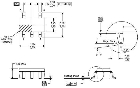
SN74LVC1G06DCKR Package

The following figure is SN74LVC1G06DCKR Package.

Package


SN74LVC1G06DCKR Manufacturer

Texas Instruments Incorporated (TI) is an American technology corporation based in Dallas, Texas, that creates and manufactures semiconductors and integrated circuits for electronic designers and manufacturers around the world. Based on sales volume, it is one of the top ten semiconductor businesses in the world. Analog chips and embedded processors, which account for more than 80% of the company's revenue, are the company's main focus. TI also makes calculators, microcontrollers, and multi-core processors, as well as TI digital light processing technologies and education technology.


Datasheet PDF

SN74LVC1G06DCKR Documents

Download datasheets and manufacturer documentation for SN74LVC1G06DCKR

Frequently Asked Questions

What is specified in the SN74LVC1G06DCKR single inverter buffer and driver?
1.65-V to 5.5-V VCC operation.
The use of the die as the package in what technology is a significant advancement in IC packaging concepts?
NanoFree package technology.
What does the SN74LVC1G06DCKR device have?
Open-drain output.
Sink current is limited to what?
32 mA.
What is the sink current required for Ioff applications?
Partial power down.
What turns off the outputs when the device is shut down?
The Ioff circuitry.
What happens when the Ioff circuitry turns off the outputs of the SN74LVC1G06DCKR device?
Stops current from flowing back into the gadget.
FAQ
What is specified in the SN74LVC1G06DCKR single inverter buffer and driver?
1.65-V to 5.5-V VCC operation.
The use of the die as the package in what technology is a significant advancement in IC packaging concepts?
NanoFree package technology.
What does the SN74LVC1G06DCKR device have?
Open-drain output.
Sink current is limited to what?
32 mA.
What is the sink current required for Ioff applications?
Partial power down.
What turns off the outputs when the device is shut down?
The Ioff circuitry.
What happens when the Ioff circuitry turns off the outputs of the SN74LVC1G06DCKR device?
Stops current from flowing back into the gadget.

TAGS

Share