ATTENTION: Due to increased demand and order volume, processing time may take an additional 1-3 business days.
HomeCommunitySubjectSN74LVC1G126DCKR Single Bus Buffer Gate: Schematic, Pinout, and Datasheet

SN74LVC1G126DCKR Single Bus Buffer Gate: Schematic, Pinout, and Datasheet

IC BUF NON-INVERT 5.5V SC70-5 The SN74LVC1G126DCKR single buffer is designed to work with a VCC voltage range of 1.65 to 3.6 volts. This article mainly introduces Schematic, Pinout, Datasheet and other detailed information about Texas Instruments SN74LVC1G126DCKR.
155

Apr 8, 2022

Darlene Sophia

Buffer Gate


IC BUF NON-INVERT 5.5V SC70-5

The SN74LVC1G126DCKR single buffer is designed to work with a VCC voltage range of 1.65 to 3.6 volts. This article mainly introduces Schematic, Pinout, Datasheet and other detailed information about Texas Instruments SN74LVC1G126DCKR.
SN74LVC1G126DCKR

492In Stock
Min.: 1 Mult.: 1
Price not displayed? Not available to buy online? Please send an RFQ, and we will respond immediately.
Quick Links

SN74LVC1G126DCKR Description

This single buffer is designed to work with a VCC voltage range of 1.65 to 3.6 volts. The SN74LVC1G126DCKR is a single-line driver having three output states. When the output-enable input is low, the output is disabled.

The SN74LVC1G126DCKR gadget performs the Boolean function  Y = A and has a dual buffer gate with output enable control.

This device is completely qualified for Ioff-based partial-power-down applications. When the device is turned off, the Ioff circuitry disables the outputs, preventing dangerous current backflow through the device.

OE should be connected to GND via a pulldown resistor to ensure a high-impedance state during power up or power down; the minimum value of the resistor is specified by the driver's current-sourcing capabilities.

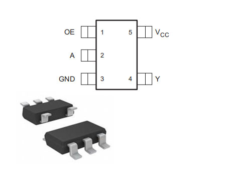
SN74LVC1G126DCKR Pinout

The following figure is SN74LVC1G126DCKR Pinout.

Pinout


Pin Number Pin Name Description
2 A A Input
3 GND Ground Pin
1 OE OE Enable/Input
5 VCC Power Pin
4 Y Y Output

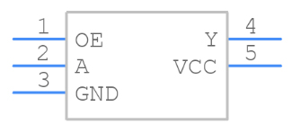
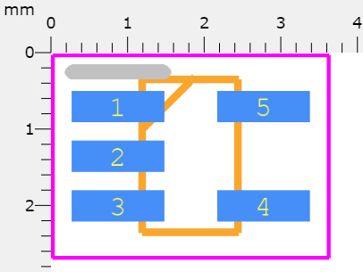
SN74LVC1G126DCKR CAD Model

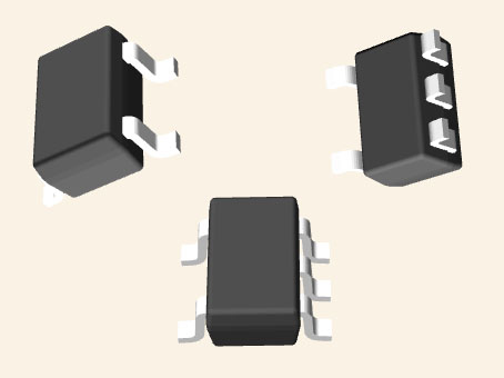
The following figures are SN74LVC1G126DCKR Symbol, Footprint and 3D Model.

Symbol

Footprint

3D Model

SN74LVC1G126DCKR Features

• Available in the  Texas Instruments  NanoFree™ Package

• Supports 5-V VCC Operation

• Inputs Accept Voltages to 5.5 V

• Provides Down Translation to VCC

• Max tpd of 3.7 ns at 3.3 V

• Low Power Consumption, 10-μA Max ICC

• ±24-mA Output Drive at 3.3 V

• Ioff Supports Live Insertion, Partial-Power-Down Mode, and Back Drive Protection

• Latch-Up  Performance Exceeds 100 mA Per JESD 78, Class II

• ESD Protection Exceeds JESD 22

– 2000-V  Human-Body Model 

– 200-V Machine Model

– 1000-V Charged-Device Model

Specifications

SN74LVC1G126DCKR Tech Specifications

Texas Instruments SN74LVC1G126DCKR technical specifications, attributes, parameters and parts with similar specifications to Texas Instruments SN74LVC1G126DCKR.
Product Attribute Attribute Value
Lifecycle StatusACTIVE (Last Updated: 5 days ago)
Factory Lead Time6 Weeks
MountSurface Mount
Mounting TypeSurface Mount
Package / Case5-TSSOP, SC-70-5, SOT-353
Number of Pins5Pins
Operating Temperature-40°C~125°C TA
PackagingTape & Reel (TR)
Series74LVC
JESD-609 Codee4
Pbfree Codeyes
Part StatusActive
Moisture Sensitivity Level (MSL)1 (Unlimited)
Number of Terminations5Terminations
TerminationSMD/SMT
ECCN CodeEAR99
Terminal FinishNickel/Palladium/Gold (Ni/Pd/Au)
Packing MethodTR
Product Attribute Attribute Value
Voltage - Supply1.65V~5.5V
Terminal PositionDUAL
Terminal FormGULL WING
Peak Reflow Temperature (Cel)260
Number of Functions1Function
Supply Voltage3.3V
Frequency100MHz
Base Part Number74LVC1G126
Pin Count5
Output Type3-State
PolarityNon-Inverting
Power Supplies3.3V
Number of Channels1Channel
Number of Ports2Ports
Nominal Supply Current10μA
Number of Bits1Bit
Propagation Delay9 ns
Quiescent Current10μA
Product Attribute Attribute Value
Turn On Delay Time9.8 ns
FamilyLVC/LCX/Z
Logic FunctionBuffer, Inverting
Number of Inputs1Input
Logic TypeBuffer, Non-Inverting
Max I(ol)0.032 A
Control TypeENABLE HIGH
Count DirectionUNIDIRECTIONAL
Schmitt Trigger InputNo
Ambient Temperature Range High125°C
Height1.1mm
Length2mm
Width1.25mm
Thickness900μm
REACH SVHCNo SVHC
RoHS StatusROHS3 Compliant
Lead FreeLead Free
0 Products View Similar

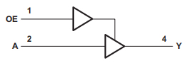
SN74LVC1G126DCKR Functional Block Diagram

The following figure is SN74LVC1G126DCKR Functional Block Diagram.

Functional Block Diagram

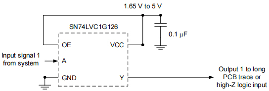
SN74LVC1G126DCKR Typical Application

The following is SN74LVC1G126DCKR Typical Application.

Typical Application

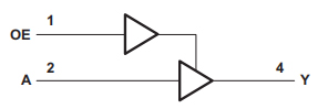
SN74LVC1G126DCKR Simplified Schematic

The SN74LVC1G126DCKR Simplified Schematic is shown as follows.

Simplified Schematic

SN74LVC1G126DCKR Layout

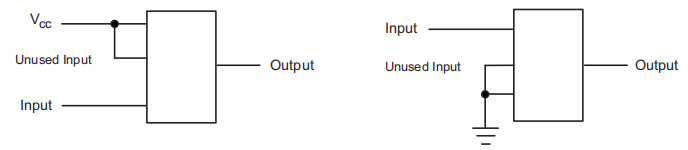
Inputs should not float while working with multiple bit logic devices. Digital logic devices often have functionalities or sections of functions that aren't utilised. When only two of a triple-input  AND gate's inputs are used, for example, or when only three of a four-buffer gate's inputs are used, these are examples. The undefined voltages at the outside connections result in undefined operating states, hence such input pins should not be kept disconnected.

The following diagram illustrates the principles that must be followed at all times. To prevent floating, all unused inputs of digital logic devices must be connected to a high or low bias. The logic level that should be applied to any given unused input is determined by the device's function. They'll usually be connected to GND or VCC, depending on which makes more sense or is handier. Floating outputs are permissible unless the part is a transceiver. If the transceiver has an output enable pin, asserting it will disable the part's outputs section. The input component of the I/Os will not be disabled, therefore they will not float when disabled.

Layout

SN74LVC1G126DCKR Alternatives

Part Number Description Manufacturer
74LVC1G126SE-7LOGIC Bus Driver, LVC/LCX/Z Series, 1-Func, 1-Bit, True Output, CMOS, PDSO5, GREEN, SOT-353, 5 PIN Diodes Incorporated
74LVC1G126GW-GLOGIC IC LVC/LCX/Z SERIES, 1-BIT DRIVER, TRUE OUTPUT, PDSO5, 1.25 MM, PLASTIC, MO-203, SC-88A, SOT353-1, TSSOP-5, Bus Driver/Transceiver NXP Semiconductors
SN74LVC1G126DCKRE4LOGIC LVC/LCX/Z SERIES, 1-BIT DRIVER, TRUE OUTPUT, PDSO5 Texas Instruments
TC7SZ126FULOGIC IC LVC/LCX/Z SERIES, 1-BIT DRIVER, TRUE OUTPUT, PDSO5, 0.65 MM PITCH, PLASTIC, SSOP-5, Bus Driver/Transceiver Toshiba America Electronic Components
935299659125LOGIC Bus Driver, LVC/LCX/Z Series, 1-Func, 1-Bit, True Output, CMOS, PDSO5 Nexperia
935268721125LOGIC IC LVC/LCX/Z SERIES, 1-BIT DRIVER, TRUE OUTPUT, PDSO5, PLASTIC, SC-88A, SOT-353, 5 PIN, Bus Driver/Transceiver NXP Semiconductors
74LVC1G126GW,165LOGIC 74LVC1G126 - Bus buffer/line driver; 3-state TSSOP 5-Pin NXP Semiconductors

SN74LVC1G126DCKR Applications

• Cable Modem Termination Systems

• High-Speed Data Acquisition and Generation

• Military: Radars and Sonars

• Motor Controls: High-Voltage

• Power Line Communication Modems

• SSDs: Internal or External

• Video Broadcasting and Infrastructure: Scalable Platforms

• Video Broadcasting: IP-Based Multi-Format Transcoders

• Video Communication Systems


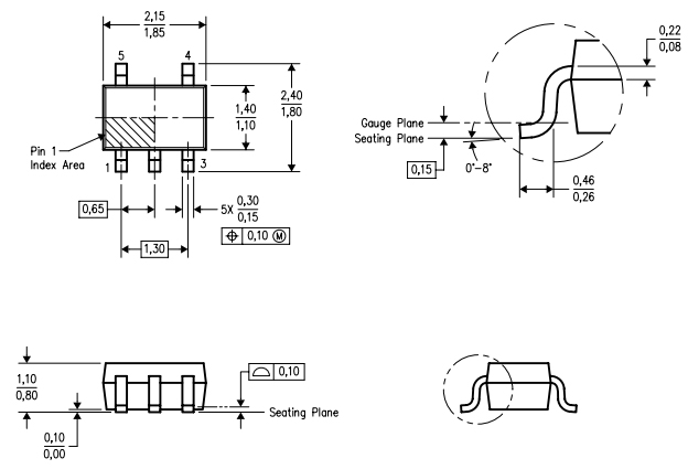
SN74LVC1G126DCKR Package

The following figure is SN74LVC1G126DCKR Package.

Package

SN74LVC1G126DCKR Manufacturer

As a global semiconductor company operating in 35 countries, Texas Instruments (TI) is first and foremost a reflection of its people. From the TIer who unveiled the first working integrated circuit in 1958 to the more than 30,000 TIers around the world today who design, manufacture and sell analog and embedded processing chips, we are problem-solvers collaborating to change the world through technology.

Datasheet PDF

SN74LVC1G126DCKR Documents

Download datasheets and manufacturer documentation for SN74LVC1G126DCKR

Frequently Asked Questions

What is the Buffer Gate?
The Buffer Gate is a logic block that takes any input and compares the value to 0. If the input signal is zero, the output will be zero. If the input is non-zero, the output will be a “1” in the bit position designated by the drop-down box. This is the opposite output result of the Zero Comparator block.
What is the difference between an NOT gate and buffer gate?
A buffer has only a single input and a single output with behavior that is the opposite of a NOT gate. It simply passes its input, unchanged, to its output. In a boolean logic simulator, a buffer is mainly used to increase propagation delay.
What is the point of a buffer gate?
Buffer gates merely serve the purpose of signal amplification: taking a “weak” signal source that isn't capable of sourcing or sinking much current, and boosting the current capacity of the signal so as to be able to drive a load. Buffer circuits are symbolized by a triangle symbol with no inverter “bubble.”
What voltage range is the single buffer designed to work with?
VCC voltage range of 1.65 to 3.6 volts.
What is a single-line driver with three output states?
SN74LVC1G126DCKR.
What does the SN74LVC1G126DCKR gadget perform?
Boolean function Y = A.
What type of applications is the SN74LVC1G126DCKR device completely qualified for?
Partial-power-down.
What disables the outputs when the device is turned off?
The Ioff circuitry.
What should OE be connected to GND via to ensure a high-impedance state during power up or power down?
A pulldown resistor.
FAQ
What is the Buffer Gate?
The Buffer Gate is a logic block that takes any input and compares the value to 0. If the input signal is zero, the output will be zero. If the input is non-zero, the output will be a “1” in the bit position designated by the drop-down box. This is the opposite output result of the Zero Comparator block.
What is the difference between an NOT gate and buffer gate?
A buffer has only a single input and a single output with behavior that is the opposite of a NOT gate. It simply passes its input, unchanged, to its output. In a boolean logic simulator, a buffer is mainly used to increase propagation delay.
What is the point of a buffer gate?
Buffer gates merely serve the purpose of signal amplification: taking a “weak” signal source that isn't capable of sourcing or sinking much current, and boosting the current capacity of the signal so as to be able to drive a load. Buffer circuits are symbolized by a triangle symbol with no inverter “bubble.”
What voltage range is the single buffer designed to work with?
VCC voltage range of 1.65 to 3.6 volts.
What is a single-line driver with three output states?
SN74LVC1G126DCKR.
What does the SN74LVC1G126DCKR gadget perform?
Boolean function Y = A.
What type of applications is the SN74LVC1G126DCKR device completely qualified for?
Partial-power-down.
What disables the outputs when the device is turned off?
The Ioff circuitry.
What should OE be connected to GND via to ensure a high-impedance state during power up or power down?
A pulldown resistor.

TAGS

Share