ATTENTION: Due to increased demand and order volume, processing time may take an additional 1-3 business days.
HomeCommunitySubjectSN74LVC2G17DCKR Dual Schmitt-Trigger Buffer: Circuit, Pinout, and Datasheet

SN74LVC2G17DCKR Dual Schmitt-Trigger Buffer: Circuit, Pinout, and Datasheet

IC BUF NON-INVERT 5.5V SC70-6 The SN74LVC2G17DCKR is a two-buffer device that performs the Y = A Boolean function. This article mainly introduces Circuit, Pinout, Datasheet and other detailed information about Texas Instruments SN74LVC2G17DCKR.

145

Mar 22, 2022

Vicky Dorothy

Understanding schmitt trigger


IC BUF NON-INVERT 5.5V SC70-6

The SN74LVC2G17DCKR is a two-buffer device that performs the Y = A Boolean function. This article mainly introduces Circuit, Pinout, Datasheet and other detailed information about Texas Instruments SN74LVC2G17DCKR.


SN74LVC2G17DCKR

853In Stock
Min.: 1 Mult.: 1
Price not displayed? Not available to buy online? Please send an RFQ, and we will respond immediately.
Quick Links

SN74LVC2G17DCKR Description

This Dual Schmitt-Trigger Buffer is rated for a VCC range of 1.65 to 5.5 volts.

The SN74LVC2G17DCKR is a two-buffer device that performs the Y = A Boolean function. The device acts as two separate buffers, but due to Schmitt action, the input threshold levels for positive (VT+) and negative (VT–) signals may differ.

The NanoFreeTM package technology, which uses the die as the package, is a major development in IC packaging technologies.

This device is completely qualified for Ioff-based partial-power-down applications. When the device is turned off, the Ioff circuitry disables the outputs, preventing dangerous current backflow through the device.

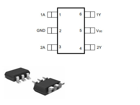
SN74LVC2G17DCKR Pinout

The following shows SN74LVC2G17DCKR Pinout.

Pinout


Pin Number Pin Name Description
1 1A Input 1
6 1Y Output 1
3 2A Input 2
4 2Y Output 2
2 GND Ground
5 VCC Power Pin

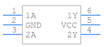
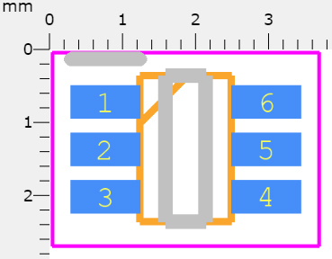
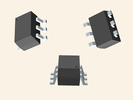
SN74LVC2G17DCKR CAD Model

The SN74LVC2G17DCKR CAD Model is shown as follows.

Symbol

Footprint

3D Model

SN74LVC2G17DCKR Features

• Available in the  Texas Instruments  NanoFree™ Package

• Supports 5-V VCC Operation

• Inputs Accept Voltages to 5.5 V

• Max tpd of 5.4 ns at 3.3 V

• Low Power Consumption, 10-μA Max ICC

• ±24-mA Output Drive at 3.3 V

• Typical VOLP (Output Ground Bounce) <0.8 V at VCC = 3.3 V, TA = 25°C

• Typical VOHV (Output VOH Undershoot) >2 V at VCC = 3.3 V, TA = 25°C

• Ioff Supports Live Insertion, Partial-Power-Down Mode Operation and Back Drive Protection

• Latch-Up Performance Exceeds 100 mA Per JESD 78, Class II

• ESD Protection Exceeds JESD 22

– 2000-V Human-Body Model (A114-A)

– 1000-V  Charged-Device Model  (C101)

Specifications

SN74LVC2G17DCKR Tech Specifications

Texas Instruments SN74LVC2G17DCKR technical specifications, attributes, parameters and parts with similar specifications to Texas Instruments SN74LVC2G17DCKR.

Product Attribute Attribute Value
Lifecycle StatusACTIVE (Last Updated: 5 days ago)
Factory Lead Time6 Weeks
Contact PlatingGold
MountSurface Mount
Mounting TypeSurface Mount
Package / Case6-TSSOP, SC-88, SOT-363
Number of Pins6Pins
Operating Temperature-40°C~125°C TA
PackagingCut Tape (CT)
Series74LVC
JESD-609 Codee4
Pbfree Codeyes
Part StatusActive
Moisture Sensitivity Level (MSL)1 (Unlimited)
Number of Terminations6Terminations
TerminationSMD/SMT
ECCN CodeEAR99
Packing MethodTR
Product Attribute Attribute Value
Voltage - Supply1.65V~5.5V
Terminal PositionDUAL
Terminal FormGULL WING
Peak Reflow Temperature (Cel)260
Number of Functions2Functions
Supply Voltage3.3V
Base Part Number74LVC2G17
Pin Count6
Output TypePush-Pull
PolarityNon-Inverting
Supply Voltage-Max (Vsup)5.5V
Power Supplies3.3V
Number of Channels2Channels
Load Capacitance50pF
Nominal Supply Current250mA
Propagation Delay4.3 ns
Quiescent Current10μA
Input TypeSchmitt Trigger
Product Attribute Attribute Value
Turn On Delay Time9.3 ns
FamilyLVC/LCX/Z
Logic FunctionBuffer, Schmitt Trigger
Number of Inputs2Inputs
Logic TypeBuffer, Non-Inverting
Number of Bits per Element1
Prop. Delay@Nom-Sup5.4 ns
Max Junction Temperature (Tj)150°C
Schmitt Trigger InputYes
Height1.1mm
Length2mm
Width1.25mm
Thickness900μm
REACH SVHCNo SVHC
Radiation HardeningNo
RoHS StatusROHS3 Compliant
Lead FreeLead Free
0 Products View Similar

N74LVC2G17DCKR Functional Block Diagram

The following figure SN74LVC2G17DCKR Functional Block Diagram.

Functional Block Diagram

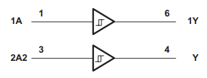
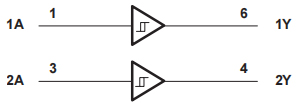
SN74LVC2G17DCKR Logic Diagram

The following shows SN74LVC2G17DCKR Logic Diagram.

Positive Logic

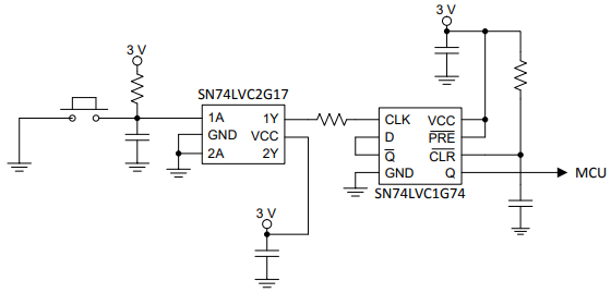
SN74LVC2G17DCKR Typical Power Button Circuit

Device Power Button Circuit

This device features a balanced output drive and is based on CMOS technologyBus congestion should be avoided at all costs because it can cause currents to exceed permissible limits. The higher drive can be achieved by combining outputs, but this will result in faster edges into mild loads, therefore routing and load circumstances should be examined to avoid ringing.

SN74LVC2G17DCKR Layout

Inputs should not float when using multiple bit logic devices. Functionalities or parts of functions of digital logic devices are frequently left unused. When only two inputs of a triple-input AND gate are used, or when only three of the four buffer gates are used, these are examples. The undefined voltages at the outside connections result in undefined operating states, hence such input pins should not be left disconnected.

The following diagram illustrates the principles that must be followed at all times. To prevent floating, all unused inputs of digital logic devices must be connected to a high or low bias. The logic level that should be applied to any given unused input is determined by the device's function. They'll usually be connected to GND or VCC, depending on which makes more sense or is more handy.

Layout

SN74LVC2G17DCKR Alternatives

Part Number Description Manufacturer
SN74LVC2G17QDCKRQ1LOGIC Automotive 2-ch, 1.65-V to 5.5-V buffers with Schmitt-Trigger inputs 6-SC70 -40 to 125 Texas Instruments
SN74LVC2G17DCKTLOGIC 2-ch, 1.65-V to 5.5-V buffers with Schmitt-Trigger inputs 6-SC70 -40 to 125 Texas Instruments
74LVC2G17GWLOGIC Buffer, LVC/LCX/Z Series, 2-Func, 1-Input, CMOS, PDSO6 Nexperia
74LVC2G17GW,125LOGIC 74LVC2G17 - Dual non-inverting Schmitt trigger with 5 V tolerant input TSSOP 6-Pin NXP Semiconductors
74LVC2G07GW-Q100,125LOGIC Buffer, LVC/LCX/Z Series, 2-Func, 1-Input, CMOS, PDSO6 Nexperia
SN74LVC2G07DCKRLOGIC 2-ch, 1.65-V to 5.5-V buffers with open-drain outputs 6-SC70 -40 to 125 Texas Instruments
SN74LVC2G07DCKRG4LOGIC 2-ch, 1.65-V to 5.5-V buffers with open-drain outputs 6-SC70 -40 to 125 Texas Instruments
SN74LVC2G17DCKTE4LOGIC 2-ch, 1.65-V to 5.5-V buffers with Schmitt-Trigger inputs 6-SC70 -40 to 125 Texas Instruments
SN74LVC2G07DCKTLOGIC 2-ch, 1.65-V to 5.5-V buffers with open-drain outputs 6-SC70 -40 to 125 Texas Instruments
74LVC2G07GWLOGIC Buffer, LVC/LCX/Z Series, 2-Func, 1-Input, CMOS, PDSO6 Nexperia

SN74LVC2G17DCKR Applications

• AV Receivers

• Audio Docks: Portable

• Blu-ray Players and  Home Theater 

• MP3 Players/Recorders

• Personal Digital Assistants (PDAs)

• Power: Telecom/Server AC/DC Supply: Single Controller: Analog and Digital

• Solid State Drives (SSDs): Client and Enterprise

• TVs: LCD/Digital and  High-Definition  (HDTVs)

• Tablets: Enterprise

• Video Analytics: Server

• Wireless Headsets, Keyboards, and Mice

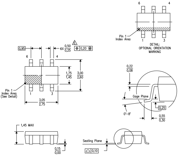
SN74LVC2G17DCKR Package

The following figure is SN74LVC2G17DCKR Package.

Package

SN74LVC2G17DCKR Manufacturer

Texas Instruments Incorporated, based in Dallas, Texas, creates and manufactures semiconductors and different integrated circuits, which it sells to electronics designers and manufacturers all over the world.


Datasheet PDF

SN74LVC2G17DCKR Documents

Download datasheets and manufacturer documentation for SN74LVC2G17DCKR

Frequently Asked Questions

What is Schmitt trigger used for?
Schmitt trigger devices are typically used in signal conditioning applications to remove noise from signals used in digital circuits, particularly mechanical contact bounce in switches.
What is the SN74LVC2G17DCKR rated for?
VCC range of 1.65 to 5.5 volts.
What does the SN74LVC2G17DCKR perform?
Y = A Boolean function.
What does the SN74LVC2G17DCKR act as?
Two separate buffers.
What is a major development in IC packaging technologies?
NanoFreeTM package technology.
What type of applications is the NanoFreeTM package technology completely qualified for?
Partial-power-down.
What disables the outputs when the device is turned off?
The Ioff circuitry.
FAQ
What is Schmitt trigger used for?
Schmitt trigger devices are typically used in signal conditioning applications to remove noise from signals used in digital circuits, particularly mechanical contact bounce in switches.
What is the SN74LVC2G17DCKR rated for?
VCC range of 1.65 to 5.5 volts.
What does the SN74LVC2G17DCKR perform?
Y = A Boolean function.
What does the SN74LVC2G17DCKR act as?
Two separate buffers.
What is a major development in IC packaging technologies?
NanoFreeTM package technology.
What type of applications is the NanoFreeTM package technology completely qualified for?
Partial-power-down.
What disables the outputs when the device is turned off?
The Ioff circuitry.

TAGS

Share