ATTENTION: Due to increased demand and order volume, processing time may take an additional 1-3 business days.
HomeCommunitySubjectSST39SF040 4 Mbit MPF: Features, Datasheet and Timing Diagram

SST39SF040 4 Mbit MPF: Features, Datasheet and Timing Diagram

Memory SST39SF040 Non-Volatile 32-LCC (J-Lead) 4Mb 512K x 8 FLASH -40°C~85°C TA 4.5V~5.5V Parallel 5V 1.27mm MICROCHIP - SST39SF040-70-4I-NHE - MEMORY, FLASH, 4MBIT, PARL, 32PLCC

91

Nov 29, 2021

Josephine Robbins

What Is Flash Memory?


Memory SST39SF040 Non-Volatile 32-LCC (J-Lead) 4Mb 512K x 8 FLASH -40°C~85°C TA 4.5V~5.5V Parallel 5V 1.27mm MICROCHIP - SST39SF040-70-4I-NHE - MEMORY, FLASH, 4MBIT, PARL, 32PLCC

The SST39SF040 is CMOS Multi-Purpose Flash (MPF) device manufactured with SST proprietary, high performance CMOS SuperFlash technology. The SST39SF040 writes (Program or Erase) with a 4.5-5.5V power supply, and conforms to JEDEC standard pinouts for x8 memories. Furthermore, Huge range of Semiconductors, Capacitors, Resistors and IcS in stock. Welcome RFQ.
SST39SF040-70-4I-NHE

2335In Stock
Min.: 1 Mult.: 1
Quantity Unit Price Ext. Price
1+ $2.59664$2.6
10+ $2.44966$24.5
100+ $2.311$231.1
500+ $2.18019$1090.1
1000+ $2.05678$2056.78
Unit Price:$2.59664
Subtotal: $2.6
Looking for a better price? Want a lower wholesale price? Please send an RFQ, and we will respond immediately.
Quick Links

SST39SF040 Pinout

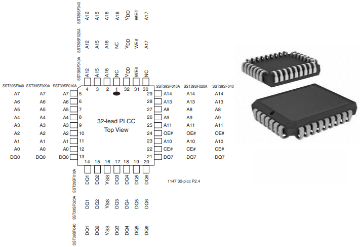
The following figure is the diagram of SST39SF040 pinout.

Pinout

SST39SF040 CAD Model

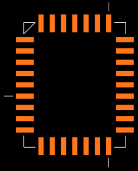
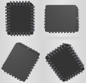
The followings are SST39SF040 Symbol, Footprint, and 3D Model.

Symbol


Footprint


3D Model

SST39SF040 Overview

The SST39SF040 is CMOS Multi-Purpose Flash (MPF) manufactured with SST's proprietary, high performance CMOS SuperFlash technology. The split-gate cell design and thick oxide tunneling injector attain better reliability and manufacturability compared with alternate approaches. The SST39SF040 device writes (Program or Erase) with a 4.5-5.5V power supply. The SST39SF040 device conforms to JEDEC standard pinouts for x8 memories. Featuring high performance Byte-Program, the SST39SF040 device provides a maximum Byte-Program time of 20 µsec. To meet high density, surface mount requirements, the SST39SF040 is offered in 32-lead PLCC package.

This article provides you with a basic overview of the SST39SF040 4 Mbit MPF, including its pin descriptions, features and specifications, etc., to help you quickly understand what SST39SF040 is.

SST39SF040 Features

● Organized as 512K x8

● Single 4.5-5.5V Read and Write Operations

● Superior Reliability

   ◆ Endurance: 100,000 Cycles (typical)

   ◆ Greater than 100 years Data Retention

● Low Power Consumption (typical values at 14 MHz)

   ◆ Active Current: 10 mA (typical)

   ◆ Standby Current: 30 µA (typical)

● Sector-Erase Capability

   ◆ Uniform 4 KByte sectors

● Fast Read Access Time:

   ◆ 55 ns

   ◆ 70 ns

● Latched Address and Data

● Automatic Write Timing

   ◆ Internal VPP Generation

● Fast Erase and Byte-Program

   ◆ Sector-Erase Time: 18 ms (typical)

   ◆ Chip-Erase Time: 70 ms (typical)

   ◆ Byte-Program Time: 14 µs (typical)

   ◆ Chip Rewrite Time: 8 seconds (typical) for SST39SF040

● End-of-Write Detection

   ◆ Toggle Bit

   ◆ Data# Polling

● TTL I/O Compatibility

● JEDEC Standard

   ◆ Flash EEPROM Pinouts and command sets

● Packages Available: 32-lead PLCC

● RoHS compliant

SST39SF040 Advantage

The SST39SF040 device is suited for applications that require convenient and economical updating of program, configuration, or data memory. For all system applications, it significantly improves performance and reliability, while lowering power consumption. It inherently uses less energy during erase and program than alternative flash technologies. The total energy consumed is a function of the applied voltage, current, and time of application. Since for any given voltage range, the SuperFlash technology uses less current to program and has a shorter erase time, the total energy consumed during any Erase or Program operation is less than alternative flash technologies. The device also improves flexibility while lowering the cost for program, data, and configuration storage applications.

The device uses Toggle Bit or Data# Polling to indicate the completion of Program operation. To protect against inadvertent write, it has on-chip hardware and Software Data Protection schemes. Designed, manufactured, and tested for a wide spectrum of applications, the device is offered with a guaranteed typical endurance of 100,000 cycles. Data retention is rated at greater than 100 years. The SuperFlash technology provides fixed Erase and Program times, independent of the number of Erase/Program cycles that have occurred. Therefore the system software or hardware does not have to be modified or de-rated as is necessary with alternative flash technologies, whose Erase and Program times increase with accumulated Erase/Program cycles.

Specifications

Microchip Technology SST39SF040-70-4I-NHE technical specifications, attributes, parameters and parts with similar specifications to Microchip Technology SST39SF040-70-4I-NHE.

SST39SF040-70-4I-NHE Tech Specifications

Microchip Technology SST39SF040-70-4I-NHE technical specifications, attributes, parameters and parts with similar specifications to Microchip Technology SST39SF040-70-4I-NHE.

Product Attribute Attribute Value
Factory Lead Time1 Weeks
Mounting TypeSurface Mount
Package / Case32-LCC (J-Lead)
Surface MountYES
Number of Pins32Pins
Memory TypesNon-Volatile
Operating Temperature-40°C~85°C TA
PackagingTube
SeriesSST39 MPF™
Published2000
JESD-609 Codee3
Pbfree Codeyes
Part StatusActive
Moisture Sensitivity Level (MSL)3 (168 Hours)
Number of Terminations32Terminations
ECCN Code3A991.B.1.A
Terminal FinishMatte Tin (Sn)
Voltage - Supply4.5V~5.5V
Product Attribute Attribute Value
Terminal PositionQUAD
Peak Reflow Temperature (Cel)245
Number of Functions1Function
Supply Voltage5V
Terminal Pitch1.27mm
Time@Peak Reflow Temperature-Max (s)40
Base Part NumberSST39SF040
Pin Count32
Operating Supply Voltage5V
Power Supplies5V
Memory Size4Mb 512K x 8
Nominal Supply Current25mA
Access Time70ns
Memory FormatFLASH
Memory InterfaceParallel
Data Bus Width8b
Organization512KX8
Write Cycle Time - Word, Page20μs
Product Attribute Attribute Value
Address Bus Width19b
Density4 Mb
Standby Current-Max0.0001A
Sync/AsyncAsynchronous
Word Size8b
Programming Voltage5V
Data PollingYES
Toggle BitYES
Command User InterfaceYES
Number of Sectors/Size128Sectors/Sizes
Sector Size4K
Height2.84mm
Length14.05mm
Width11.51mm
REACH SVHCNo SVHC
Radiation HardeningNo
RoHS StatusROHS3 Compliant
Lead FreeLead Free
0 Products View Similar

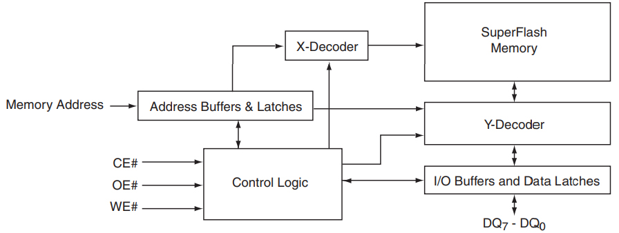
SST39SF040 Functional Block Diagram

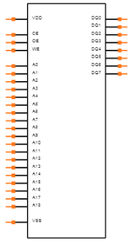
The following is the Functional Block Diagram of SST39SF040.

Functional Block Diagram

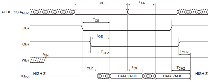
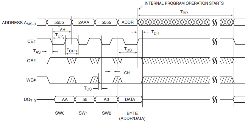
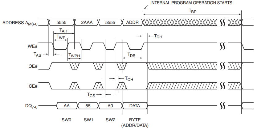
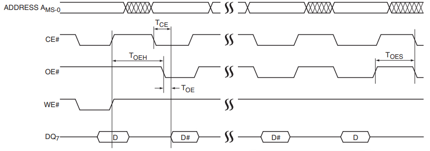
SST39SF040 Timing Diagram

The following diagram shows the SST39SF040 Timing Diagram.

Read Cycle Timing Diagram


CE# Controlled Program Cycle Timing Diagram


Data# Polling Timing Diagram


WE# Controlled Program Cycle Timing Diagram


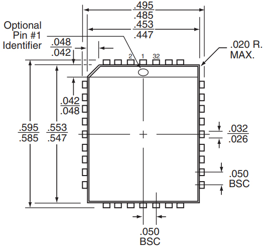
SST39SF040 Package

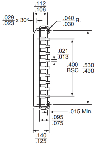
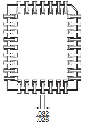
The following diagram shows the SST39SF040 package.

Top View


Side View


Bottom View

SST39SF040 Manufacturer

Microchip Technology Inc. is a leading provider of microcontroller and analog semiconductors, providing low-risk product development, lower total system cost and faster time to market for thousands of diverse customer applications worldwide. Headquartered in Chandler, Arizona, Microchip offers outstanding technical support along with dependable delivery and quality.


Datasheet PDF

SST39SF040-70-4I-NHE Documents

Download datasheets and manufacturer documentation for SST39SF040-70-4I-NHE

Frequently Asked Questions

How is SST39SF040 programmed?
The SST39SF040 is programmed on a byte-by-byte basis.
What are the advantages of the Chip-Erase operation provided by SST39SF040?
The SST39SF040 provides Chip-Erase operation, which allows the user to erase the entire memory array to the “1s” state. This is useful when the entire device must be quickly erased.
In order to optimize the system's Write cycle time, how many software means does SST39SF040 provide to detect the completion of Write (Program or Erase) cycles?
The SST39SF040 provides two software means to detect the completion of a Write (Program or Erase) cycle, in order to optimize the system Write cycle time.
What features does SST39SF040 provide to protect non-volatile data from accidental writes?
The SST39SF040 provides both hardware and software features to protect nonvolatile data from inadvertent writes.
What about SST39SF040's Program and Erasure?
The SST39SF040 provides the JEDEC approved Software Data Protection scheme for all data alteration operations, i.e., Program and Erase.
FAQ
How is SST39SF040 programmed?
The SST39SF040 is programmed on a byte-by-byte basis.
What are the advantages of the Chip-Erase operation provided by SST39SF040?
The SST39SF040 provides Chip-Erase operation, which allows the user to erase the entire memory array to the “1s” state. This is useful when the entire device must be quickly erased.
In order to optimize the system's Write cycle time, how many software means does SST39SF040 provide to detect the completion of Write (Program or Erase) cycles?
The SST39SF040 provides two software means to detect the completion of a Write (Program or Erase) cycle, in order to optimize the system Write cycle time.
What features does SST39SF040 provide to protect non-volatile data from accidental writes?
The SST39SF040 provides both hardware and software features to protect nonvolatile data from inadvertent writes.
What about SST39SF040's Program and Erasure?
The SST39SF040 provides the JEDEC approved Software Data Protection scheme for all data alteration operations, i.e., Program and Erase.

TAGS

Share