ATTENTION: Due to increased demand and order volume, processing time may take an additional 1-3 business days.
HomeCommunitySubjectSTM32F407ZGT6 Microcontroller: Feature, Pinout and Datasheet

STM32F407ZGT6 Microcontroller: Feature, Pinout and Datasheet

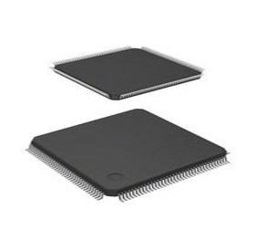
32 Bit Microcontroller, Ethernet MAC, Camera Interface, ARM Cortex-M4, 168 MHz, 1 MB, 196 KB, 144 This article mainly covers mechanical device characteristics of the STM32F407ZGT6 line of microcontroller. Furthermore, Huge range of Semiconductors, Capacitors, Resistors and IcS in stock. Welcome RFQ.

184

Sep 26, 2021

Maxine Watt

32 Bit Microcontroller, Ethernet MAC, Camera Interface, ARM Cortex-M4, 168 MHz, 1 MB, 196 KB, 144

This article mainly covers mechanical device characteristics of the STM32F407ZGT6 line of microcontroller. Furthermore, Huge range of Semiconductors, Capacitors, Resistors and IcS in stock. Welcome RFQ.

STM32F407ZGT6

4710In Stock
Min.: 1 Mult.: 1
Quantity Unit Price Ext. Price
1+ $11.27834$11.28
10+ $10.63994$106.4
100+ $10.03768$1003.77
500+ $9.46951$4734.76
1000+ $8.9335$8933.5
Unit Price:$11.27834
Subtotal: $11.28
Looking for a better price? Want a lower wholesale price? Please send an RFQ, and we will respond immediately.
Quick Links

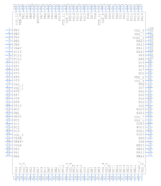
STM32F407ZGT6 Pinout

STM32F407ZGT6 CAD Model

Symbol


Footprint


3D Model

STM32F407ZGT6 Overview

The STM32F407ZGT6 is based on the high-performance ARM® Cortex®-M4 32-bit RISC core operating at a frequency of up to 168 MHz. The Cortex-M4 core features a Floating point unit (FPU) single precision which supports all ARM singleprecision data-processing instructions and data types. It also implements a full set of DSP instructions and a memory protection unit (MPU) which enhances application security.

The STM32F407ZGT6 incorporates high-speed embedded memories (Flash memory up to 1 Mbyte, up to 192 Kbytes of SRAM), up to 4 Kbytes of backup SRAM, and an extensive range of enhanced I/Os and peripherals connected to two APB buses, three AHB buses and a 32-bit multi-AHB bus matrix. In the following articles, we will have a more detailed understanding of STM32F407ZGT6 model.

STM32F407ZGT6 Features

• Core: ARM® 32-bit Cortex®-M4 CPU with FPU, Adaptive real-time accelerator (ART Accelerator™) allowing 0-wait state execution from Flash memory, frequency up to 168 MHz, memory protection unit, 210 DMIPS/1.25 DMIPS/MHz (Dhrystone 2.1), and DSP instructions

• Memories

• Up to 1 Mbyte of Flash memory

• Up to 192+4 Kbytes of SRAM including 64-Kbyte of CCM (core coupled memory) data RAM

• Flexible static memory controller supporting Compact Flash, SRAM, PSRAM, NOR and NAND memories

• LCD parallel interface, 8080/6800 modes

• Clock, reset and supply management

– 1.8 V to 3.6 V application supply and I/Os

– POR, PDR, PVD and BOR

– 4-to-26 MHz crystal oscillator

– Internal 16 MHz factory-trimmed RC (1% accuracy)

– 32 kHz oscillator for RTC with calibration

– Internal 32 kHz RC with calibration

• Low-power operation

– Sleep, Stop and Standby modes

– VBAT supply for RTC, 20×32 bit backup registers + optional 4 KB backup SRAM

• 3×12-bit, 2.4 MSPS A/D converters: up to 24 channels and 7.2 MSPS in triple interleaved mode

• 2×12-bit D/A converters

• General-purpose DMA: 16-stream DMA controller with FIFOs and burst support

• Up to 17 timers: up to twelve 16-bit and two 32-bit timers up to 168 MHz, each with up to 4 IC/OC/PWM or pulse counter and quadrature (incremental) encoder input

• Debug mode

– Serial wire debug (SWD) & JTAG interfaces

– Cortex-M4 Embedded Trace Macrocell™

• Up to 140 I/O ports with interrupt capability

– Up to 136 fast I/Os up to 84 MHz

– Up to 138 5 V-tolerant I/Os

• Up to 15 communication interfaces

– Up to 3 × I2C interfaces (SMBus/PMBus)

– Up to 4 USARTs/2 UARTs (10.5 Mbit/s, ISO 7816 interface, LIN, IrDA, modem control)

– Up to 3 SPIs (42 Mbits/s), 2 with muxed full-duplex I2S to achieve audio class accuracy via internal audio PLL or external clock

– 2 × CAN interfaces (2.0B Active)

– SDIO interface

• Advanced connectivity

– USB 2.0 full-speed device/host/OTG controller with on-chip PHY

– USB 2.0 high-speed/full-speed device/host/OTG controller with dedicated DMA, on-chip full-speed PHY and ULPI

– 10/100 Ethernet MAC with dedicated DMA: supports IEEE 1588v2 hardware, MII/RMII

• 8- to 14-bit parallel camera interface up to 54 Mbytes/s

• True random number generator

• CRC calculation unit

• 96-bit unique ID

• RTC: subsecond accuracy, hardware calendar

STM32F407ZGT6 Advantage

The STM32F407ZGT6 is part of the STM32F4 family. They are fully pinto-pin, software and feature compatible with the STM32F2xx devices, allowing the user to try different memory densities, peripherals, and performances (FPU, higher frequency) for a greater degree of freedom during the development cycle.

The STM32F407ZGT6 operates in the –40 to +105 ℃ temperature range from a 1.8 to 3.6 V power supply. The supply voltage can drop to 1.7 V when the device operates in the 0 to 70 ℃ temperature range using an external power supply supervisor: refer to Section: Internal reset OFF. A comprehensive set of power-saving mode allows the design of low-power applications.

The STM32F407ZGT6 device maintains a close compatibility with the whole STM32F10xxx family. All functional pins are pin-to-pin compatible. The STM32F407ZGT6, however, are not drop-in replacements for the STM32F10xxx devices: the two families do not have the same power scheme, and so their power pins are different. Nonetheless, transition from the STM32F10xxx to the STM32F40xxx family remains simple as only a few pins are impacted.

Specifications

STM32F407ZGT6 Tech Specifications

STMicroelectronics STM32F407ZGT6 technical specifications, attributes, parameters and parts with similar specifications to STMicroelectronics STM32F407ZGT6.

Product Attribute Attribute Value
Lifecycle StatusACTIVE (Last Updated: 7 months ago)
Factory Lead Time12 Weeks
Mounting TypeSurface Mount
Package / Case144-LQFP
Surface MountYES
Number of Pins144Pins
Data ConvertersA/D 24x12b; D/A 2x12b
Number of I/Os114I/Os
Watchdog TimersYes
Operating Temperature-40°C~85°C TA
PackagingTray
SeriesSTM32F4
Part StatusActive
Moisture Sensitivity Level (MSL)3 (168 Hours)
Number of Terminations144Terminations
Terminal PositionQUAD
Terminal FormGULL WING
Supply Voltage3.3V
Product Attribute Attribute Value
Terminal Pitch0.5mm
Frequency168MHz
Base Part NumberSTM32F407
Pin Count144
InterfaceCAN, EBI/EMI, Ethernet, I2C, I2S, IrDA, LIN, SPI, UART, USART, USB
Memory Size1MB
Oscillator TypeInternal
RAM Size192K x 8
Voltage - Supply (Vcc/Vdd)1.8V~3.6V
uPs/uCs/Peripheral ICs TypeMICROCONTROLLER, RISC
Core ProcessorARM® Cortex®-M4
PeripheralsBrown-out Detect/Reset, DMA, I2S, LCD, POR, PWM, WDT
Program Memory TypeFLASH
Core Size32-Bit
Program Memory Size1MB 1M x 8
ConnectivityCANbus, DCMI, EBI/EMI, Ethernet, I2C, IrDA, LINbus, SPI, UART/USART, USB OTG
Bit Size32
Has ADCYES
Product Attribute Attribute Value
DMA ChannelsYES
Data Bus Width32b
Number of Timers/Counters14Timers/Counters
Core ArchitectureARM
CPU FamilyCORTEX-M4
Number of ADC Channels24ADC Channels
Number of PWM Channels2PWM Channels
Number of I2C Channels3I2C Channels
Number of Ethernet Channels1Ethernet Channel
Height1.45mm
Length20.2mm
Width20.2mm
REACH SVHCNo SVHC
Radiation HardeningNo
RoHS StatusROHS3 Compliant
Lead FreeLead Free
0 Products View Similar

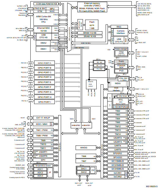
STM32F407ZGT6 Functional Block Diagram

block diagram

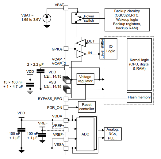
Power supply scheme

STM32F407ZGT6 Thermal Characteristics

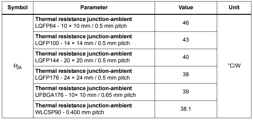
The maximum chip-junction temperature, TJ max, in degrees Celsius, may be calculated

using the following equation:

TJ max = TA max + (PD max x ΘJA)

Where:

• TA max is the maximum ambient temperature in ℃,

• ΘJA is the package junction-to-ambient thermal resistance, in ℃/W,

• PD max is the sum of PINT max and PI/O max (PD max = PINT max + PI/Omax),

• PINT max is the product of IDD and VDD, expressed in Watts. This is the maximum chip internal power.

PI/O max represents the maximum power dissipation on output pins where:

PI/O max = Σ (VOL × IOL) + Σ((VDD – VOH) × IOH),

taking into account the actual VOL / IOL and VOH / IOH of the I/Os at low and high level in the application.

Package thermal characteristics

STM32F407ZGT6 Equivalent

        Model number          Manufacturer                                            Description
STM32F205RGT7TR      STMicroelectronics 32-BIT, FLASH, 120MHz, RISC MICROCONTROLLER, PQFP64, 10 X 10 MM, ROHS COMPLIANT, LQFP-64
STM32F205RGT6W      STMicroelectronics High-performance Arm Cortex-M3 MCU with 1 Mbyte of Flash memory, 120 MHz CPU, ART Accelerator
STM32F205RGT6TR      STMicroelectronics High-performance Arm Cortex-M3 MCU with 1 Mbyte of Flash memory, 120 MHz CPU, ART Accelerator
STM32F407ZGT6XXX      STMicroelectronics 32-BIT, FLASH, 168MHz, RISC MICROCONTROLLER, PQFP144, 20 X 20 MM, 0.50  MM PITCH, ROHS COMPLIANT, LQFP-144
STM32F205RGT6XXX      STMicroelectronics 32-BIT, FLASH, 120MHz, RISC MICROCONTROLLER, PQFP64, 10 X 10 MM, ROHS COMPLIANT, LQFP-64
STM32F205RGT6      STMicroelectronics High-performance Arm Cortex-M3 MCU with 1 Mbyte of Flash memory, 120 MHz CPU, ART Accelerator
STM32F205RGT7      STMicroelectronics High-performance Arm Cortex-M3 MCU with 1 Mbyte of Flash memory, 120 MHz CPU, ART Accelerator
STM32F407ZGT7      STMicroelectronics High-performance foundation line, Arm Cortex-M4 core with DSP and FPU, 1 Mbyte of Flash memory, 168 MHz CPU, ART Accelerator, Ethernet, FSMC
STM32F205RGT7XXX      STMicroelectronics 32-BIT, FLASH, 120MHz, RISC MICROCONTROLLER, PQFP64, 10 X 10 MM, ROHS COMPLIANT, LQFP-64
STM32F407ZGT7TR      STMicroelectronics 32-BIT, FLASH, 168MHz, RISC MICROCONTROLLER, PQFP144, 20 X 20 MM, 0.50 MM PITCH, ROHS COMPLIANT, LQFP-144

STM32F407ZGT6 Application

• Motor drive and application control

• Medical equipment

• Industrial applications: PLC, inverters, circuit breakers

• Printers, and scanners

• Alarm systems, video intercom, and HVAC

• Home audio appliances


STM32F407ZGT6 Package

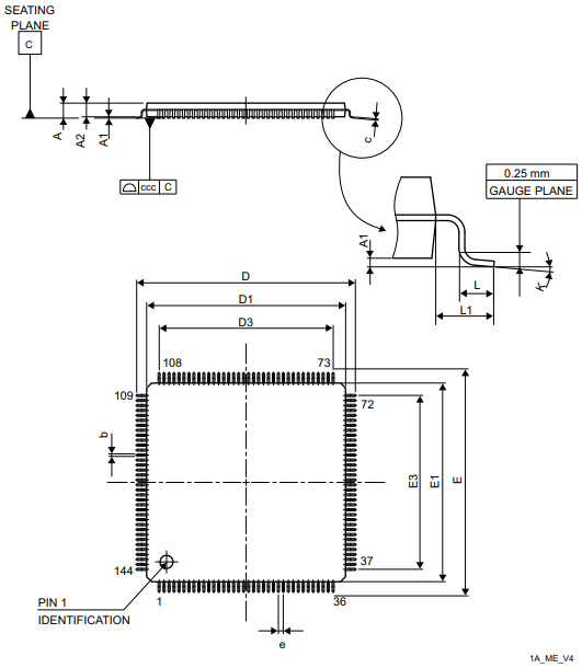
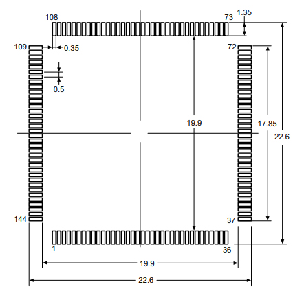
LQFP144 package outline

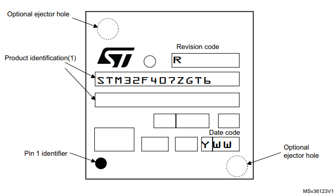
LQFP144 marking example (package top view)

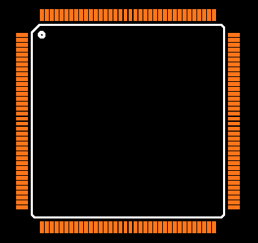
LQFP144 package recommended footprint

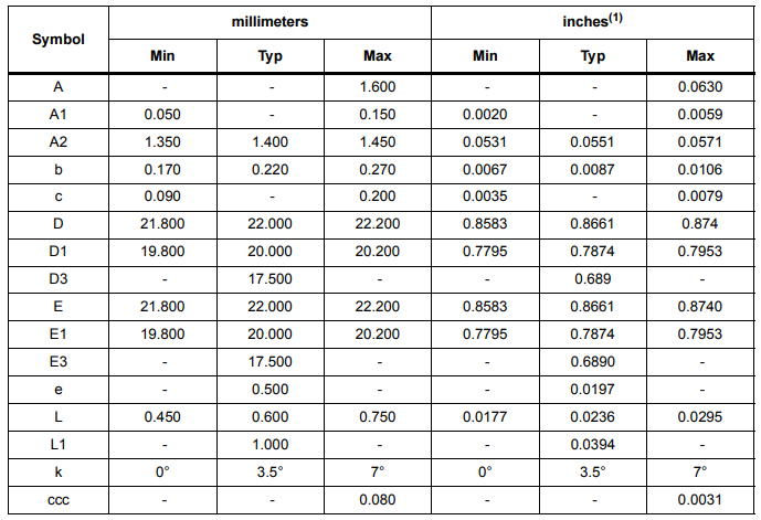
LQFP144  package mechanical data

STM32F407ZGT6 Manufacturer

STMicroelectronics is a globally recognized semiconductor company. They are dedicated to developing semiconductor solutions for various microelectronics applications. STMicroelectronics enjoys unrivaled silicon and system expertise, strong manufacturing strength, IP portfolio,and solid relationships with their strategic partners. Based on these advantages, STMicroelectronics has become a pioneer in System-on-Chip (SoC) technology and its products has a positive effect in realizing today's convergence trends.

Datasheet PDF

STM32F407ZGT6 Documents

Download datasheets and manufacturer documentation for STM32F407ZGT6

Frequently Asked Questions

What three low-power modes does the STM32F407ZGT6 support to achieve the best compromise between low-power consumption, short startup time and available wakeup sources?
Sleep mode, Stop mode and Standby mode.
How many timers does STM32F407ZGT6 device contain?
The STM32F407ZGT6 includes two advanced-control timers, eight general-purpose timers, two basic timers and two watchdog timers.
In the STM32F407ZGT6 device, how many synchronizable general-purpose timers are there?
There are ten synchronizable general-purpose timers embedded in the STM32F407ZGT6 device.
What effect does the Memory Protection Unit (MPU) have on STM32F407ZGT6?
The Memory Protection Unit (MPU) is used to manage the CPU accesses to memory to prevent one task to accidentally corrupt the memory or resources used by any other active task. The MPU is especially helpful for applications where some critical or certified code has to be protected against the misbehavior of other tasks.
FAQ
What three low-power modes does the STM32F407ZGT6 support to achieve the best compromise between low-power consumption, short startup time and available wakeup sources?
Sleep mode, Stop mode and Standby mode.
How many timers does STM32F407ZGT6 device contain?
The STM32F407ZGT6 includes two advanced-control timers, eight general-purpose timers, two basic timers and two watchdog timers.
In the STM32F407ZGT6 device, how many synchronizable general-purpose timers are there?
There are ten synchronizable general-purpose timers embedded in the STM32F407ZGT6 device.
What effect does the Memory Protection Unit (MPU) have on STM32F407ZGT6?
The Memory Protection Unit (MPU) is used to manage the CPU accesses to memory to prevent one task to accidentally corrupt the memory or resources used by any other active task. The MPU is especially helpful for applications where some critical or certified code has to be protected against the misbehavior of other tasks.

TAGS

Share