ATTENTION: Due to increased demand and order volume, processing time may take an additional 1-3 business days.
HomeCommunitySubjectSTP55NF06 Power MOSFET: Pinout, Datasheet, Equivalent

STP55NF06 Power MOSFET: Pinout, Datasheet, Equivalent

Transistors - FETs, MOSFETs - Single Trans MOSFET N-CH 60V 50A 3-Pin(3+Tab) TO-220 Tube

3663

Nov 26, 2021

Morgan Davy

N-Channel MOSFET as a Switch. Turn ON a 12V Motor with Arduino.


Transistors - FETs, MOSFETs - Single Trans MOSFET N-CH 60V 50A 3-Pin(3 Tab) TO-220 Tube

The STP55NF06 MOSFET is an N-channel power MOSFET. This article will cover its pinout, datasheet, equivalent and more detailed information about STP55NF06. Welcome your RFQ!


STP55NF06

238In Stock
Min.: 1 Mult.: 1
Price not displayed? Not available to buy online? Please send an RFQ, and we will respond immediately.
Quick Links

The overview of STP55NF06

The STP55NF06 MOSFET  is an N-channel power MOSFET with a wide range of applications. This MOSFET is notable for its high drain current and fast switching speed, as well as its low on-resistance, which boosts the device's efficiency. According to the datasheet, this MOSFET will begin to conduct at a low gate voltage of 10V, but it will reach its maximum drain current at a gate voltage of 20V. This MOSFET can be driven by a microcontroller or a logic-level device because it is designed for high-power applications.

Because this MOSFET has a low gate threshold voltage of only 4V, it can be turned on using just 5V from a GPIO pin on a microcontroller like the  Arduino. However, this does not imply that the MOSFET will come on completely with just 5V; it requires roughly 10V to switch on completely and deliver a continuous current of 27A. If you're looking for a MOSFET to utilize with a microcontroller, logic-level MOSFETs like the 2N7002 or IRLZ44N are a good choice. Alternatively, you can use a transistor and a driver circuit to provide 10V to the gate pin of this MOSFET. The frequency response of this MOSFET is quite good hence it can be used in DC-DC converter circuits also.

Because the MOSFET is made up of a capacitor, there will be no voltage in the gate under normal circumstances and without external influence, which is why we need to pull the gate of the MOSFET to the ground to prevent false triggering of the circuit. As we all know, MOSFETs are voltage-controlled devices, which means that to turn them off, we only need to provide voltage to the gate and no current should flow through the MOSFET.

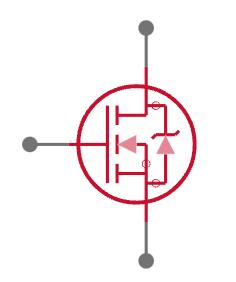
STP55NF06 CAD Model

STP55NF06 Symbol


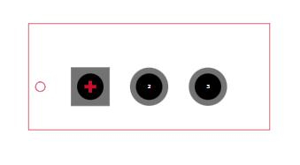
STP55NF06 Footprint


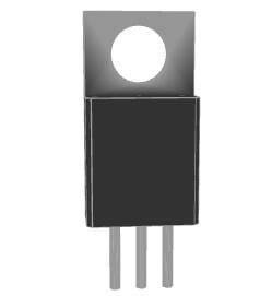
STP55NF06 3D Model

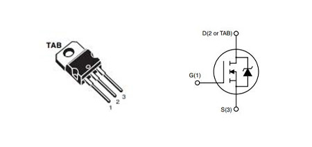
STP55NF06 Pinout

STP55NF06 Feature

  • N-Channel Power MOSFET

  • Continuous Drain Current (ID): 35A

  • Pulsed Drain Current (ID-peak) is 50A

  • Drain to Source Breakdown Voltage: 60V

  • Drain Source Resistance (RDS) is 0.018 Ohms

  • The gate threshold voltage (VGS-th) is 20V (max)

  • Rise time and the fall time is 50nS and 15nS

  • Input Capacitance 1300pF

  • Output Capacitance 300pF

  • Available in To-220 package

STP55NF06 Application

  • Use in Electric Power Steering (EPS)

  • Use in Anti-locking Braking System (ABS)

  • Use in Wiper Control

  • Use in Climate Control

  • Use in Power Door

STP55NF06 Test Circuit

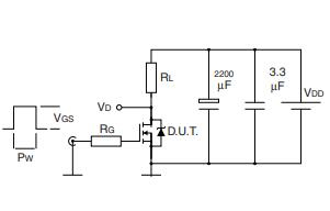
The following figure shows the test circuit of STP55NF06:

STP55NF06-Switching times test circuit for resistive load

STP55NF06-Gate charge test circuit

How to Use STP55NF06 MOSFET?

Because MOSFETs are voltage-controlled devices, only a minimum voltage is required to switch them on. The gate turn-on voltage for the STP55NF06 MOSFET is just 4V because it is an N-channel MOSFET, which means it will be on when the MOSFET's gate is linked to the supply's  VCC  and off when it is pulled down or connected to the ground.

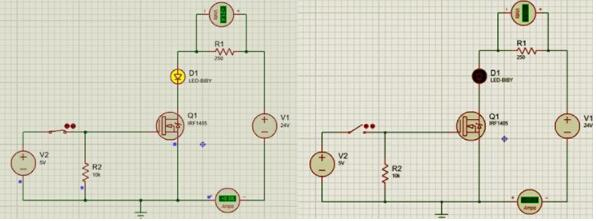
The simulated circuit below shows how this MOSFET operates when the basic circuit's gate is connected to the ground and when the power supply's VCC is connected to it.

 STP55NF06 Circuit

When we connect the gate to the supply to switch on the MOSFET, it will stay on until the gate voltage of the MOSFET falls below the threshold voltage of the MOSFET. This voltage is less than 4V for this STP55NF06 MOSFET; below this voltage, the MOSFET will be in its ohmic state, and no current will flow through the device. As previously stated, the gate of the MOSFET should be linked to the ground using a pull-down resistor. In the example circuit, a 10K resistor is used to pull down the MOSFET's gate to the ground.

Specifications

STMicroelectronics STP55NF06 technical specifications, attributes, parameters and parts with similar specifications to STMicroelectronics STP55NF06.

STP55NF06 Tech Specifications

STMicroelectronics STP55NF06 technical specifications, attributes, parameters and parts with similar specifications to STMicroelectronics STP55NF06.

Product Attribute Attribute Value
Lifecycle StatusACTIVE (Last Updated: 8 months ago)
Factory Lead Time12 Weeks
MountThrough Hole
Mounting TypeThrough Hole
Package / CaseTO-220-3
Number of Pins3Pins
Weight4.535924g
Transistor Element MaterialSILICON
Current - Continuous Drain (Id) @ 25℃50A Tc
Drive Voltage (Max Rds On, Min Rds On)10V
Number of Elements1 Element
Power Dissipation (Max)110W Tc
Turn Off Delay Time36 ns
Operating Temperature-55°C~175°C TJ
PackagingTube
SeriesSTripFET™ II
JESD-609 Codee3
Part StatusActive
Moisture Sensitivity Level (MSL)1 (Unlimited)
Product Attribute Attribute Value
Number of Terminations3Terminations
ECCN CodeEAR99
Resistance18mOhm
Terminal FinishMatte Tin (Sn)
Voltage - Rated DC60V
Current Rating50A
Base Part NumberSTP55N
Pin Count3
Element ConfigurationSingle
Operating ModeENHANCEMENT MODE
Power Dissipation30W
Turn On Delay Time20 ns
FET TypeN-Channel
Transistor ApplicationSWITCHING
Rds On (Max) @ Id, Vgs18m Ω @ 27.5A, 10V
Vgs(th) (Max) @ Id4V @ 250μA
Input Capacitance (Ciss) (Max) @ Vds1300pF @ 25V
Gate Charge (Qg) (Max) @ Vgs60nC @ 10V
Rise Time50ns
Product Attribute Attribute Value
Vgs (Max)±20V
Fall Time (Typ)15 ns
Continuous Drain Current (ID)50A
Threshold Voltage3V
JEDEC-95 CodeTO-220AB
Gate to Source Voltage (Vgs)20V
Drain Current-Max (Abs) (ID)55A
Drain to Source Breakdown Voltage60V
Pulsed Drain Current-Max (IDM)200A
Dual Supply Voltage60V
Nominal Vgs3 V
Height9.15mm
Length10.4mm
Width4.6mm
REACH SVHCNo SVHC
Radiation HardeningNo
RoHS StatusROHS3 Compliant
Lead FreeLead Free
0 Products View Similar

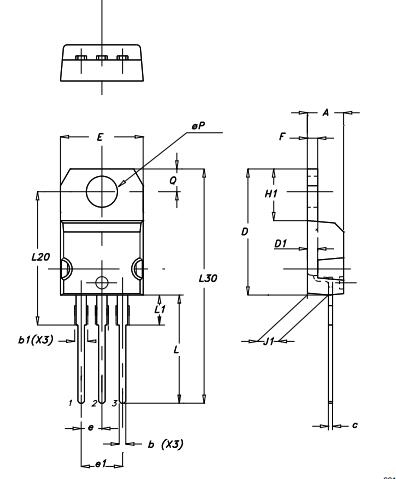
STP55NF06 Package

STP55NF06 Package

STP55NF06 Manufacturer

STMicroelectronics is a global independent semiconductor company and is a leader in developing and delivering semiconductor solutions across the spectrum of microelectronics applications. An unrivalled combination of silicon and system expertise, manufacturing strength, Intellectual Property (IP) portfolio and strategic partners positions the Company at the forefront of System-on-Chip (SoC) technology and its products play a key role in enabling today's convergence trends.

Datasheet PDF

Download datasheets and manufacturer documentation for STMicroelectronics STP55NF06.

STP55NF06 Documents

Download datasheets and manufacturer documentation for STP55NF06

TAGS

Share