ATTENTION: Due to increased demand and order volume, processing time may take an additional 1-3 business days.
HomeCommunitySubjectTCA9548APWR I2C Switch: Circuit, Pinout, and Datasheet

TCA9548APWR I2C Switch: Circuit, Pinout, and Datasheet

IC I2C SW 8CH W/RESET 24TSSOP The TCA9548APWR is a bidirectional translating I2C switch with eight channels. This article mainly introduces Circuit, Pinout, Datasheet and other detailed information about Texas Instruments TCA9548APWR.

3479

Mar 1, 2022

Mag Caroline

TCA9548A I2C Multiplexer: Use Multiple Devices with the Same Address on Arduino


IC I2C SW 8CH W/RESET 24TSSOP

The TCA9548APWR is a bidirectional translating I2C switch with eight channels. This article mainly introduces Circuit, Pinout, Datasheet and other detailed information about Texas Instruments TCA9548APWR.

TCA9548APWR

641In Stock
Min.: 1 Mult.: 1
Price not displayed? Not available to buy online? Please send an RFQ, and we will respond immediately.
Quick Links

TCA9548APWR Description

The TCA9548APWR is a bidirectional translating  I2C  switch with eight channels. SC0/SD0-SC7/SD7 are the slave devices that receive the master SCL/SDA signal pair. Any of the eight downstream channels, as well as any combination of them, can be chosen.

The TCA9548APWR includes an active-low RESET input that resets the state machine and helps the device to recover if one of the downstream I2C buses becomes stuck in a low state. The device's state machine can also be reset by cycling the power supply, commonly known as a power-on reset, by cycling the power supply, VCC (POR). All channels are deselected when you use the RESET function or a POR.

The I2C data path connections are controlled by a single I2C master device that can communicate with numerous I2C slaves. After the slave address (hardware selectable by A0, A1, and A2 pins) is successfully acknowledged, a single 8-bit control register is written to or read from to determine the preferred channels.

The TCA9548APWR can also be used for voltage translation, letting 1.8-V, 2.5-V, or 3.3-V parts interact with 5-V parts by using various bus voltages on each SCn/SDn pair. External pull-up resistors are used to bring the bus up to the desired voltage for both the master and slave channels.

TCA9548APWR Pinout

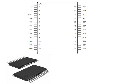
The following figure shows TCA9548APWR Pinout.

Pinout


Pin Number Pin Name Description
1 A0 Address input 0. Connect directly to VCC or ground
2 A1 Address input 1. Connect directly to VCC or ground
21 A2 Address input 2. Connect directly to VCC or ground
12 GND Ground
3 RESET Active-low reset input. Connect to VCC or VDPUM through a pull-up resistor, if not used
4 SD0 Serial data 0. Connect to VDPU0 through a pull-up resistor
5 SC0 Serial clock 0. Connect to VDPU0 through a pull-up resistor
6 SD1 Serial data 1. Connect to VDPU1 through a pull-up resistor
7 SC1 Serial clock 1. Connect to VDPU1 through a pull-up resistor
8 SD2 Serial data 2. Connect to VDPU2 through a pull-up resistor
9 SC2 Serial clock 2. Connect to VDPU2 through a pull-up resistor
10 SD3 Serial data 3. Connect to VDPU3 through a pull-up resistor
11 SC3 Serial clock 3. Connect to VDPU3 through a pull-up resistor
13 SD4 Serial data 4. Connect to VDPU4 through a pull-up resistor
14 SC4 Serial clock 4. Connect to VDPU4 through a pull-up resistor
15 SD5 Serial data 5. Connect to VDPU5 through a pull-up resistor
16 SC5 Serial clock 5. Connect to VDPU5 through a pull-up resistor
17 SD6 Serial data 6. Connect to VDPU6 through a pull-up resistor
18 SC6 Serial clock 6. Connect to VDPU6 through a pull-up resistor
19 SD7 Serial data 7. Connect to VDPU7 through a pull-up resistor
20 SC7 Serial clock 7. Connect to VDPU7 through a pull-up resistor
22 SCL Serial clock bus. Connect to VDPUM through a pull-up resistor
23 SDA Serial data bus. Connect to VDPUM through a pull-up resistor
24 VCC Supply voltage

TCA9548APWR CAD Model

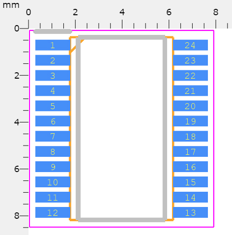
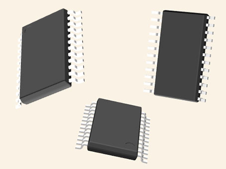
The followings are TCA9548APWR Symbol, Footprint and 3D Model.

Symbol

Footprint

3D Model

TCA9548APWR Features

• Pin savings on the I2C master, as each switch is activated or isolated through the I2C software

• Supports voltage-level translation for any bus voltages in the range of 1.65 V-5.5 V which is essential in mixed voltage I2C systems

• 1-to-8 Bidirectional translating switches

• I2C Bus and  SMBus  compatible

• Active-low reset input

• Three address pins, allowing up to eight TCA9548A devices on the I2C bus

• Channel selection through an I2C Bus, in any combination

• Power up with all switch channels deselected

• Low RON switches

• Allows voltage-level translation between 1.8-V, 2.5-V, 3.3-V, and 5-V buses

• No glitch on power up

• Supports hot insertion

• Low standby current

• Operating power-supply voltage range of 1.65 V to 5.5 V

• 5-V Tolerant inputs

• 0- to 400-kHz Clock frequency

• Latch-up performance exceeds 100 mA Per JESD 78, class II

•  ESD Protection  exceeds JESD 22

– ±2000-V Human-body model (A114-A)

– 200-V Machine model (A115-A)

– ±1000-V Charged-device model (C101)

Specifications

TCA9548APWR Tech Specifications

Texas Instruments TCA9548APWR technical specifications, attributes, parameters and parts with similar specifications to Texas Instruments TCA9548APWR.

Product Attribute Attribute Value
Lifecycle StatusACTIVE (Last Updated: 4 days ago)
Factory Lead Time12 Weeks
Contact PlatingGold
MountSurface Mount
Mounting TypeSurface Mount
Package / Case24-TSSOP (0.173, 4.40mm Width)
Number of Pins24Pins
Operating Temperature-40°C~85°C
PackagingCut Tape (CT)
SeriesTCA
JESD-609 Codee4
Pbfree Codeyes
Part StatusActive
Moisture Sensitivity Level (MSL)1 (Unlimited)
Number of Terminations24Terminations
ECCN CodeEAR99
Product Attribute Attribute Value
TypeBus Switch
Resistance70Ohm
Additional FeatureALSO OPERATES AT VCC 2.3V TO 3.6V
Packing MethodTR
Voltage - Supply1.65V~5.5V
Terminal PositionDUAL
Terminal FormGULL WING
Peak Reflow Temperature (Cel)260
Number of Functions1Function
Supply Voltage1.8V
Terminal Pitch0.65mm
Time@Peak Reflow Temperature-Max (s)NOT SPECIFIED
Base Part NumberCA9548
Number of Outputs8Outputs
Circuit1 x 8:1
Supply Voltage-Max (Vsup)5.5V
Product Attribute Attribute Value
InterfaceI2C, SMBus
Load Capacitance50pF
Max Supply Current80μA
Supply TypeSingle
Output PolarityTRUE
Power Supply Current-Max (ICC)0.08mA
Voltage Supply SourceSingle Supply
Independent Circuits1
Ambient Temperature Range High85°C
Height1.2mm
Length7.8mm
Width4.4mm
Thickness1mm
REACH SVHCNo SVHC
RoHS StatusROHS3 Compliant
Lead FreeLead Free
0 Products View Similar

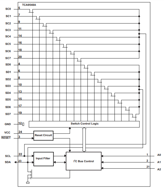
TCA9548APWR Functional Block Diagram

The TCA9548APWR Functional Block Diagram is shown as follows.

Functional Block Diagram

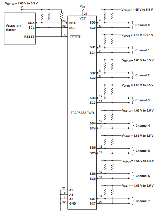
TCA9548APWR Typical Application

The following figure shows an application in which the TCA9548APWR can be used.

Typical Application

One or more data pull-up voltages, VDPUX, are used in a typical TCA9548APWR application, one for the master device (VDPUM) and one for each of the configurable slave channels (VDPU0 – VDPU7). VDPUM = VDPUX = VCC if the master device and all slave devices are both powered by the same voltage. Additional design criteria must be considered when determining an adequate VCC voltage in an application where voltage translation is required.

The slave address of the TCA9548APWR is controlled via the A0, A1, and A2 pins, which are hardware configurable. In some applications, these ports can be connected directly to GND or VCC.

If the application activates numerous slave channels at the same time, the total IOL from SCL/SDA to GND on the master side equals the sum of the currents through all pull-up resistors, Rp.

The TCA9548APWR's pass-gate transistors are designed in such a way that the VCC voltage can be used to limit the maximum voltage that can be transmitted from one I2C bus to the next.

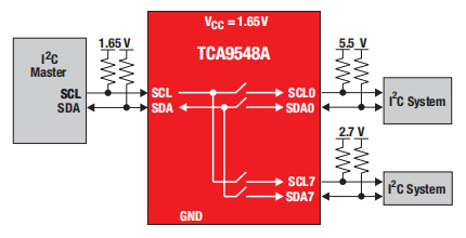
TCA9548APWR Circuit Diagram

The I2C multiplexer/switch shown in this diagram allows I2C systems to grow while keeping the two-wire bus basic. It also has the ability to do voltage translation and segment isolation.

Dual bidirectional translating switch controlled via I2C bus


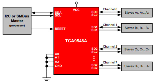
TCA9548APWR Simplified Application Diagram

The following figure is TCA9548APWR Simplified Application Diagram.

Simplified Application Diagram

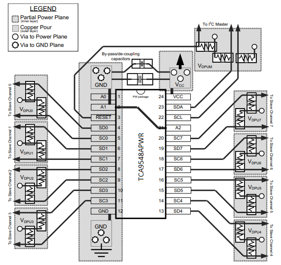
TCA9548APWR Layout

Common PCB layout principles must be followed for the TCA9548APWR's PCB layout, but additional considerations connected to high-speed data transfer, such as matching impedances and differential pairs, are not an issue for I2C signal speeds. A dedicated ground plane on an inner layer of the board is typical, and ground-connected pins must have a low-impedance path to the ground plane in the form of large polygon pours and many vias. To manage the voltage on the VCC pin, by-pass and de-coupling capacitors are typically employed, with a larger capacitor providing more power in the event of a short power supply glitch and a smaller capacitor filtering out high-frequency ripple.

Layout

All VDPUX voltages and VCC might be at the same potential in an application where voltage translation isn't necessary, and a single copper plane could link all of the pull-up resistors to the proper reference voltage. VDPUM and VDPU0 – VDPU7 may all be on the same layer of the board with split planes to separate distinct voltage potentials in an application where voltage translation is necessary.

Data lines (SCn and  SDn ) must be as short as feasible, and trace widths must be kept to a minimum (for example, 5-10 mils depending on copper weight) to reduce overall I2C bus capacitance added by PCB parasitics.

TCA9548APWR Alternatives

Part Number Description Manufacturer
PCA9548PW-TDRIVERS AND INTERFACES IC 9548 SERIES, 8 LINE TO 1 LINE MULTIPLEXER, TRUE OUTPUT, PDSO24, 4.40 MM, PLASTIC, SOT-355-1, MO-153, TSSOP-24, Multiplexer/Demultiplexer NXP Semiconductors
PCA9548APWG4DRIVERS AND INTERFACES 9548 SERIES, 8 LINE TO 1 LINE MULTIPLEXER, TRUE OUTPUT, PDSO24, GREEN, PLASTIC, TSSOP-24 Texas Instruments
PCA9548APW,112DRIVERS AND INTERFACES PCA9548A - 8-channel I²C-bus switch with reset TSSOP2 24-Pin NXP Semiconductors
PCA9548PWMICROCONTROLLERS AND PROCESSORS Bus Controller, PDSO24 Philips Semiconductors

TCA9548APWR Applications

• Resolves I2C address conflicts

• I2C bus isolation

• I2C bus expansion

• Servers

• Routers (telecom switching equipment)

• Factory automation

• Products with I2C slave address conflicts (such as multiple, identical temperature sensors)

• Communications & Networking

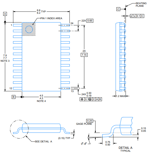
TCA9548APWR Package

The following figure is TCA9548APWR Package.

Package

TCA9548APWR Manufacturer

Texas Instruments Incorporated (TI) is a Texas-based technology company that designs and manufactures semiconductors and integrated circuits for electronic designers and manufacturers all over the world. It is one of the top ten semiconductor companies in the world based on sales volume. The company's major focus is analog chips and embedded processors, which account for more than 80% of the company's sales. Calculators, microcontrollers, and multi-core processors, as well as TI digital light processing technologies and education technology, are all manufactured by TI.


Datasheet PDF

TCA9548APWR Documents

Download datasheets and manufacturer documentation for TCA9548APWR

Frequently Asked Questions

What is TCA9548A?
The TCA9548A device has eight bidirectional translating switches that can be controlled through the I2C bus. The SCL/SDA upstream pair fans out to eight downstream pairs, or channels.
How do I reset TCA9548A?
The system master can reset the TCA9548A in the event of a time-out or other improper operation by asserting a low in the RESET input. Similarly, the power-on reset deselects all channels and initializes the I2C/SMBus state machine.
How many channels does the TCA9548APWR have?
Eight.
What are the slave devices that receive the master SCL/SDA signal pair?
SC0/SD0-SC7/SD7.
How many downstream channels can be chosen?
Any of the eight downstream channels.
What type of input does the TCA9548APWR include?
Active-low RESET input.
What is the power supply commonly known as?
Power-on reset.
How are the I2C data path connections controlled?
Single I2C master device.
What is the TCA9548APWR used for?
Voltage translation.
What is used to bring the bus up to the desired voltage for both the master and slave channels?
External pull-up resistors.
FAQ
What is TCA9548A?
The TCA9548A device has eight bidirectional translating switches that can be controlled through the I2C bus. The SCL/SDA upstream pair fans out to eight downstream pairs, or channels.
How do I reset TCA9548A?
The system master can reset the TCA9548A in the event of a time-out or other improper operation by asserting a low in the RESET input. Similarly, the power-on reset deselects all channels and initializes the I2C/SMBus state machine.
How many channels does the TCA9548APWR have?
Eight.
What are the slave devices that receive the master SCL/SDA signal pair?
SC0/SD0-SC7/SD7.
How many downstream channels can be chosen?
Any of the eight downstream channels.
What type of input does the TCA9548APWR include?
Active-low RESET input.
What is the power supply commonly known as?
Power-on reset.
How are the I2C data path connections controlled?
Single I2C master device.
What is the TCA9548APWR used for?
Voltage translation.
What is used to bring the bus up to the desired voltage for both the master and slave channels?
External pull-up resistors.

TAGS

Share