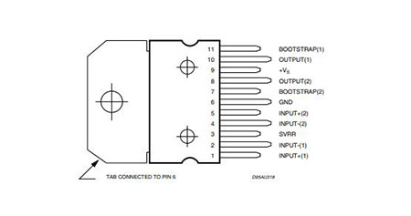
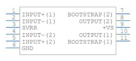
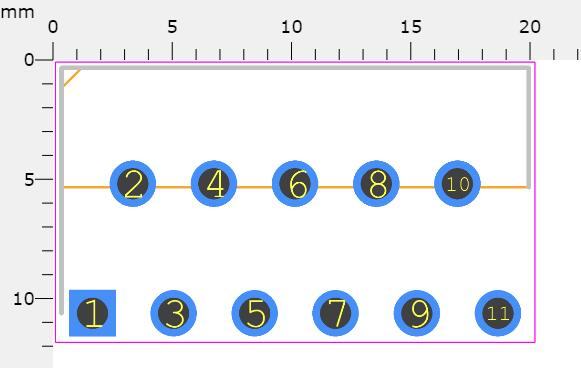
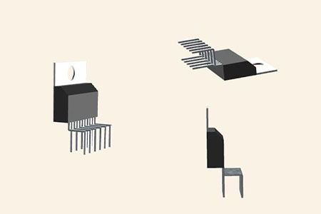
First and foremost, the circuit receives voltage. The voltage will then be charged to C5 via D1. The voltage increases at IC1/1's pin 10 (output). Until the voltage of the power supply is about identical.
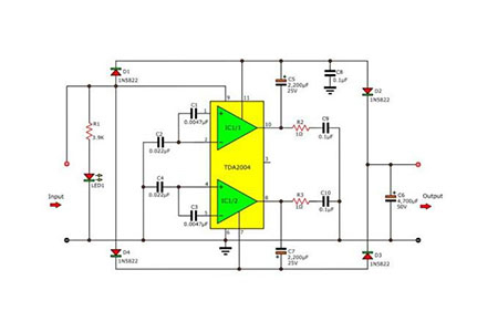
Circuit diagram of step-up DC converter using TDA2004
D2 then transmits the electricity to C6 to charge it. It results in a voltage of roughly 0V at pin 10 of IC1/1. However, the voltage across C6 or the output is about equivalent to the power supply.
Following that, the voltage on the output (pin 8) of IC1/2 begins to climb. Because C5 has ceased to charge. As a result, C7 is charged via the power supply.
As a result, there is a current pass D3 to charge C6. And the voltage at pin 8 is around 0V.
The circuit's operation will thereafter be restarted in the same manner as before.
At C6, both the current get out of pin 8 and the current get out of pin 10 will be combined.
As a result, the output voltage rises to 2 times the input voltage. Because the input voltages of pins 8 and 10 are mixed together.
The capacitors C1 through C4 function as a 5 kHz square wave generator. To figure out how IC1 works.