ATTENTION: Due to increased demand and order volume, processing time may take an additional 1-3 business days.
HomeCommunitySubjectTPS1H000AQDGNRQ1 High-Side Switch: Circuit, Pinout, and Datasheet

TPS1H000AQDGNRQ1 High-Side Switch: Circuit, Pinout, and Datasheet

The TPS1H000AQDGNRQ1 is a smart high-side switch that has an internal charge pump and a single-channel NMOS power FET. This article mainly introduces Circuit, Pinout, Datasheet and other detailed information about Texas Instruments TPS1H000AQDGNRQ1.

158

Mar 25, 2022

Glenn Lawson

Transistor as a switch - low side or high side


The TPS1H000AQDGNRQ1 is a smart high-side switch that has an internal charge pump and a single-channel NMOS power FET. This article mainly introduces Circuit, Pinout, Datasheet and other detailed information about Texas Instruments TPS1H000AQDGNRQ1.

TPS1H000AQDGNRQ1

958In Stock
Min.: 1 Mult.: 1
Price not displayed? Not available to buy online? Please send an RFQ, and we will respond immediately.
Quick Links

TPS1H000AQDGNRQ1 Description

The TPS1H000AQDGNRQ1 is a smart high-side switch that has an internal charge pump and a single-channel NMOS power FET. The configurable current-limit mechanism considerably improves the system's overall reliability. The load may be intelligently controlled thanks to full diagnostic features.

Setting the current-limit value for the application is possible with the external high-accuracy current limit. When there is an overcurrent, the device increases system reliability by effectively clamping the inrush current. By decreasing the size of PCB traces and connectors, as well as the capacity of the previous power stage, the TPS1H000AQDGNRQ1 device can cut system costs. When a current limit is reached, the TPS1H000AQDGNRQ1 device has three modes. Users can adjust the output to one of three modes by configuring the DELAY pin: hold the current consistently, latch off instantly, or retry automatically. The design flexibility provided by the customizable behaviors during current limit addresses functionality, cost, and thermal dissipation.

With the digital status output, the TPS1H000AQDGNRQ1 device offers full diagnostics. Real-time on-state monitoring is possible thanks to high-accuracy and low-threshold open-load detection. The TPS1H000AQDGNRQ1 device also offers a standalone mode, which allows the system to implement complete functionality locally without the use of an MCU.

The TPS1H000AQDGNRQ1 is a smart high-side switch that can be used to control a wide range of resistive, inductive, and capacitive loads, such as LEDs, relays, and sub-modules.

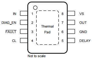
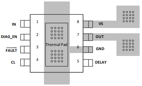
TPS1H000AQDGNRQ1 Pinout

The following is TPS1H000AQDGNRQ1 Pinout.

Pinout


Pin Number Pin Name Description
4 CL Adjustable current limit. Connect to device GND if external current limit is not used
5 DELAY Function configuration when in current limit; internal pullup
2 DIAG_EN Enable the diagnostic function
3 FAULT Open-drain diagnostic status output. Leave floating if not used
6 GND Ground pin
1 IN Input control for output activation; internal pulldown
7 OUT Output, source of the high-side switch, connected to the load
8 VS Power supply, drain for the high-side switch
  Thermal pad Thermal pad. Connect to device GND or leave floating.

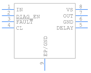
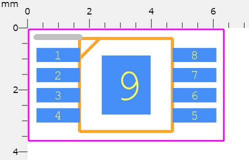
TPS1H000AQDGNRQ1 CAD Model

The following shows TPS1H000AQDGNRQ1 CAD Model.

Symbol

Footprint

3D Model

TPS1H000AQDGNRQ1 Features

• Qualified for Automotive Applications

• AEC-Q100 Qualified With the Following Results:

– Device Temperature Grade 1: –40°C to 125°C

 Ambient Operating Temperature Range

– Device HBM ESD Classification Level H2

– Device CDM ESD Classification Level C4B

• Single-Channel 1000-mΩ Smart High-Side Switch

• Wide Operating Voltage: 3.4 V to 40 V • Low Standby Current: <500 nA

• Adjustable Current Limit With External Resistor

– ±15% When ≥150 mA

– ±10% When ≥300 mA

• Configurable Behavior After Current Limit

– Holding Mode

– Latch-Off Mode With Adjustable Delay Time

– Auto-Retry Mode

• Supports Standalone Operation Without an MCU

• Protection:

– Short-to-GND and Overload

– Thermal Shutdown and Thermal Swing 

– Negative Voltage Clamp for Inductive Loads

– Loss-of-GND and Loss-of-Battery

• Diagnostics:

– Overload and Short-to-GND Detection

– Open-Load and Short-to-Battery Detection in ON or OFF State

– Thermal Shutdown and Thermal Swing

Specifications

TPS1H000AQDGNRQ1 Tech Specifications

Texas Instruments TPS1H000AQDGNRQ1 technical specifications, attributes, parameters and parts with similar specifications to Texas Instruments TPS1H000AQDGNRQ1.

Product Attribute Attribute Value
Lifecycle StatusACTIVE (Last Updated: 3 days ago)
Factory Lead Time6 Weeks
Mounting TypeSurface Mount
Package / Case8-TSSOP, 8-MSOP (0.118, 3.00mm Width) Exposed Pad
Surface MountYES
Number of Pins8Pins
Operating Temperature-40°C~125°C
PackagingTape & Reel (TR)
SeriesAutomotive, AEC-Q100
Pbfree Codeyes
Part StatusActive
Moisture Sensitivity Level (MSL)2 (1 Year)
Number of Terminations8Terminations
ECCN CodeEAR99
Terminal PositionDUAL
Terminal FormGULL WING
Product Attribute Attribute Value
Peak Reflow Temperature (Cel)NOT SPECIFIED
Number of Functions1Function
Supply Voltage13.5V
Terminal Pitch0.65mm
Time@Peak Reflow Temperature-Max (s)NOT SPECIFIED
Base Part NumberTPS1H000
Number of Outputs1Output
Output TypeN-Channel
Supply Voltage-Min (Vsup)4V
InterfaceOn/Off
Output ConfigurationHigh Side
Output Current1A
Voltage - Supply (Vcc/Vdd)Not Required
Input TypeNon-Inverting
Switch TypeRelay, Solenoid Driver
Nominal Input Voltage40V
Product Attribute Attribute Value
Ratio - Input:Output1:1
Voltage - Load4V~40V
Fault ProtectionCurrent Limiting (Fixed), Over Temperature
Turn On Time90 µs
Output Peak Current Limit-Nom1A
Rds On (Typ)1 Ω
Max Junction Temperature (Tj)150°C
Turn Off Time90 µs
Built-in ProtectionsTRANSIENT; OVER CURRENT; THERMAL; UNDER VOLTAGE
FeaturesSlew Rate Controlled
Height1.1mm
Length3mm
Width3mm
Thickness1.02mm
RoHS StatusROHS3 Compliant
0 Products View Similar

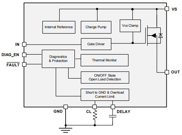
TPS1H000AQDGNRQ1 Functional Block Diagram

The following figure is TPS1H000AQDGNRQ1 Functional Block Diagram.

Functional Block Diagram

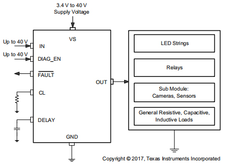
TPS1H000AQDGNRQ1 Typical Block Diagram

The following figure shows TPS1H000AQDGNRQ1 Typical Block Diagram.

Typical Block Diagram

TPS1H000AQDGNRQ1 Layout

TJ must be less than 175°C to avoid thermal shutdown. The power dissipation may be significant if the output current is quite high. The  PCB  layout, on the other hand, is critical. A good PCB design can improve heat transfer, which is critical for the device's long-term durability.

• Increase the heat conductivity of the board by increasing the copper covering on the PCB. The copper on the PCB is the primary heatflow channel from the package to the ambient. When there are no heat sinks attached to the PCB on the opposite side of the board from the package, maximum copper is critical.

• To improve the board's thermal conductivity, place as many thermal vias as feasible right beneath the package thermal pad.

• To avoid solder voids, all thermal vias should be plated shut or plugged and sealed on both sides of the board. Solder coverage should be at least 85% to assure reliability and performance.

Layout

TPS1H000AQDGNRQ1 Typical Application

The following figure shows an example of how to design the external circuitry parameters.

Typical Application Circuitry

• The VVS ranges from 6 to 18 volts.

• 100 mA nominal current.

• A current limit of 500 mA is expected.

• When a thermally sensitive system reaches its current limit, the output latches off after 0.2 seconds. The 0.2 s is used to provide a safe start-up for a capacitive load by clamping the inrush current but not latching it off.

• On-state open-load detection, short-to-GND or overcurrent detection, and thermal shutdown detection are all available with the 5-V MCU.


TPS1H000AQDGNRQ1 Applications

• Single-Channel LED Driver

• Single-Channel High-Side Relay Driver

• Body Lighting

• Advanced Driver Assistance Systems (ADAS) Sensors

• General Resistive, Inductive and Capacitive Loads

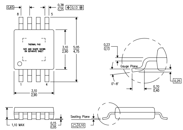
TPS1H000AQDGNRQ1 Package

The following figure is TPS1H000AQDGNRQ1 Package.

Package

TPS1H000AQDGNRQ1 Manufacturer

Texas Instruments (TI), a multinational semiconductor business with operations in 35 countries, is first and foremost a reflection of its employees. We are problem-solvers cooperating to transform the world via technology, from the TIer who introduced the first functional integrated circuit in 1958 to the more than 30,000 TIers throughout the world today who develop, build, and distribute analog and embedded processor chips.


Datasheet PDF

TPS1H000AQDGNRQ1 Documents

Download datasheets and manufacturer documentation for TPS1H000AQDGNRQ1

Frequently Asked Questions

What does the TPS1H000AQDGNRQ1 have?
NMOS power FET.
What greatly improves the systems overall reliability?
The configurable current-limit mechanism.
What can the load be controlled by the TPS1H000AQDGNRQ1?
Full diagnostic features.
How does the TPS1H000AQDGNRQ1 improve system reliability?
The inrush current.
How many modes does the TPS1H000AQDGNRQ1 have when a current limit is reached?
Three.
What does the TPS1H000AQDGNRQ1 device use to adjust the output to one of three modes?
DELAY pin.
What is the design flexibility of the TPS1H000AQDGNRQ1 device?
Customizable behaviors.
What does the TPS1H000AQDGNRQ1 offer with the digital status output?
Full diagnostics.
What is possible thanks to high-accuracy and low-threshold open-load detection?
Real-time on-state monitoring.
What does the TPS1H000AQDGNRQ1 device offer?
Standalone mode.
FAQ
What does the TPS1H000AQDGNRQ1 have?
NMOS power FET.
What greatly improves the systems overall reliability?
The configurable current-limit mechanism.
What can the load be controlled by the TPS1H000AQDGNRQ1?
Full diagnostic features.
How does the TPS1H000AQDGNRQ1 improve system reliability?
The inrush current.
How many modes does the TPS1H000AQDGNRQ1 have when a current limit is reached?
Three.
What does the TPS1H000AQDGNRQ1 device use to adjust the output to one of three modes?
DELAY pin.
What is the design flexibility of the TPS1H000AQDGNRQ1 device?
Customizable behaviors.
What does the TPS1H000AQDGNRQ1 offer with the digital status output?
Full diagnostics.
What is possible thanks to high-accuracy and low-threshold open-load detection?
Real-time on-state monitoring.
What does the TPS1H000AQDGNRQ1 device offer?
Standalone mode.

TAGS

Share