ATTENTION: Due to increased demand and order volume, processing time may take an additional 1-3 business days.
HomeCommunitySubjectTPS2051CDBVR Power-Distribution Switches: Layout, Pinout, and Datasheet

TPS2051CDBVR Power-Distribution Switches: Layout, Pinout, and Datasheet

The TPS2051CDBVR power-distribution switch series is designed for applications like USB that are prone to experience heavy capacitive loads and short circuits. This article mainly introduces Layout, Pinout, Datasheet and other detailed information about Texas Instruments TPS2051CDBVR.
125

Apr 8, 2022

Lynn Hume

Active Current Limiting Circuit Schematic


The TPS2051CDBVR power-distribution switch series is designed for applications like USB that are prone to experience heavy capacitive loads and short circuits. This article mainly introduces Layout, Pinout, Datasheet and other detailed information about Texas Instruments TPS2051CDBVR.
TPS2051CDBVR

26766In Stock
Min.: 1 Mult.: 1
Quantity Unit Price Ext. Price
1+ $6.3$6.3
10+ $4.48$44.8
25+ $4.012$100.3
100+ $3.499$349.9
250+ $3.2556$813.9
500+ $3.1088$1554.4
1000+ $2.9878$2987.8
Unit Price:$2.9878
Subtotal: $2.99
Looking for a better price? Want a lower wholesale price? Please send an RFQ, and we will respond immediately.
Quick Links

TPS2051CDBVR Description

The TPS2051CDBVR power-distribution switch series is designed for applications like USB that are prone to experience heavy capacitive loads and short circuits. Multiple devices in this family have set current-limit limits for applications ranging from 0.5 A to 2 A.

When the output load exceeds the current limit threshold, the TPS2051CDBVR family operates in a constant-current mode, limiting the output current to a safe level. This ensures a consistent fault current under all circumstances. When the output is shorted, the fast overload response time reduces the demand on the main 5-V supply, allowing it to provide regulated power. To reduce current surges during turnon and turnoff, the rise and fall times of the power switch are managed.

TPS2051CDBVR Pinout

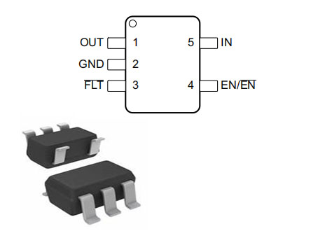
The following figure is TPS2051CDBVR Pinout.

Pinout


Pin Number Pin Name Description
4 EN/EN Enable input, logic high turns on power switch
3 FLT Active-low open-drain output, asserted during overcurrent, or overtemperature conditions
2 GND Ground connection
5 IN Input voltage and power-switch drain; connect a 0.1-µF or greater ceramic capacitor from IN to GND close to the IC
1 OUT Power-switch output, connect to load.

TPS2051CDBVR CAD Model

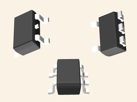
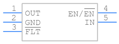
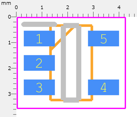
The followings are TPS2051CDBVR Symbol, Footprint and 3D Model.

Symbol

Footprint

3D Model

TPS2051CDBVR Features

• Single Power Switch Family

• Pin-for-Pin With Existing TI Switch Portfolio

• Rated Currents of 0.5 A, 1 A, 1.5 A, 2 A

• ±20% Accurate, Fixed,  Constant Current Limit 

• Fast Overcurrent Response: 2 µs

• Deglitched Fault Reporting

• Selected Parts With TPS2051CDBVR

• Reverse Current Blocking

• Built-In  Soft Start 

• Ambient Temperature Range: –40°C to 85°C

• UL Listed and CB-File No. E169910

Specifications

TPS2051CDBVR Tech Specifications

Texas Instruments TPS2051CDBVR technical specifications, attributes, parameters and parts with similar specifications to Texas Instruments TPS2051CDBVR.
Product Attribute Attribute Value
Lifecycle StatusACTIVE (Last Updated: 3 days ago)
Factory Lead Time6 Weeks
MountSurface Mount
Mounting TypeSurface Mount
Package / CaseSC-74A, SOT-753
Number of Pins5Pins
Operating Temperature-40°C~125°C TJ
PackagingDigi-Reel®
JESD-609 Codee4
Pbfree Codeyes
Part StatusActive
Moisture Sensitivity Level (MSL)2 (1 Year)
Number of Terminations5Terminations
ECCN CodeEAR99
Resistance97mOhm
Terminal FinishNickel/Palladium/Gold (Ni/Pd/Au)
Terminal PositionDUAL
Product Attribute Attribute Value
Terminal FormGULL WING
Peak Reflow Temperature (Cel)260
Number of Functions1Function
Supply Voltage5V
Base Part NumberTPS2051
Pin Count5
Output TypeN-Channel
InterfaceOn/Off
Analog IC - Other TypeANALOG CIRCUIT
Nominal Supply Current90μA
Output ConfigurationHigh Side
Output Current500mA
Voltage - Supply (Vcc/Vdd)Not Required
Input TypeNon-Inverting
Switch TypeUSB Switch
Number of Voltages Monitored1
Nominal Input Voltage5.5V
Product Attribute Attribute Value
Threshold Voltage1.45V
Ratio - Input:Output1:1
Voltage - Load4.5V~5.5V
Fault ProtectionCurrent Limiting (Fixed), Over Temperature, Reverse Current, UVLO
Rds On (Typ)97m Ω
Max Junction Temperature (Tj)125°C
Ambient Temperature Range High85°C
FeaturesLoad Discharge, Status Flag
Height1.45mm
Length2.9mm
Width1.6mm
Thickness1.2mm
REACH SVHCNo SVHC
Radiation HardeningNo
RoHS StatusROHS3 Compliant
Lead FreeLead Free
0 Products View Similar

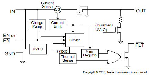
TPS2051CDBVR Functional Block Diagram

The TPS2051CDBVR Functional Block Diagram is shown as follows.

Functional Block Diagram

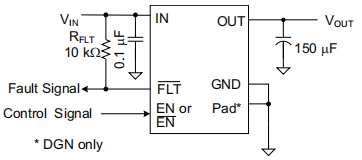
TPS2051CDBVR Typical Application Diagram

The following shows TPS2051CDBVR Typical Application Diagram.

Typical Application Diagram

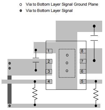
TPS2051CDBVR Layout

1. Connect the IN and  GND  pins with a low-inductance trace, and place the 100-nF bypass capacitor near the IN and GND pins.

2. Install a 10-µF low ESR ceramic capacitor near the OUT and GND pins, then connect them with a low inductance trace.

3. A wide and short copper trace must be used to link the PowerPAD to the PCB ground plane.

Layout

TPS2051CDBVR Alternatives

Part Number Description Manufacturer
TPS2051CDBVTPOWER CIRCUITS 0.5A loading, 4.5-5.5V, 97mΩ USB power switch, active-high, output discharge, reverse blocking 5-SOT-23 -40 to 125 Texas Instruments

TPS2051CDBVR Applications

• USB Ports and Hubs, Laptops, and Desktops

• High-Definition Digital TVs

• Set-Top Boxes

• Short-Circuit Protection


TPS2051CDBVR Package

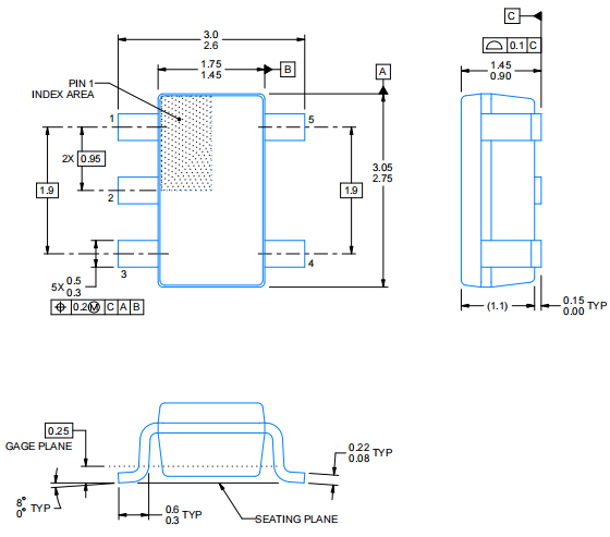
The TPS2051CDBVR Package is shown as follows.

Package

TPS2051CDBVR Manufacturer

Texas Instruments Incorporated, based in Dallas, Texas, creates and manufactures semiconductors and different integrated circuits, which it sells to electronics designers and manufacturers all over the world.

Datasheet PDF

TPS2051CDBVR Documents

Download datasheets and manufacturer documentation for TPS2051CDBVR

Frequently Asked Questions

What is the TPS2051CDBVR power-distribution switch series designed for?
USB.
What are the current limit limits for the TPS2051CDBVR power-distribution switch series?
0.5 A to 2 A.
What mode does the TPS2051CDBVR family operate in?
Constant-current mode.
What does the TPS2051CDBVR family ensure under all circumstances?
Consistent fault current.
What reduces the demand on the main 5-V supply?
The fast overload response time.
What is managed by the TPS2051CDBVR to reduce current surges during turnon and turnoff?
Rise and fall times.
FAQ
What is the TPS2051CDBVR power-distribution switch series designed for?
USB.
What are the current limit limits for the TPS2051CDBVR power-distribution switch series?
0.5 A to 2 A.
What mode does the TPS2051CDBVR family operate in?
Constant-current mode.
What does the TPS2051CDBVR family ensure under all circumstances?
Consistent fault current.
What reduces the demand on the main 5-V supply?
The fast overload response time.
What is managed by the TPS2051CDBVR to reduce current surges during turnon and turnoff?
Rise and fall times.

TAGS

Share