ATTENTION: Due to increased demand and order volume, processing time may take an additional 1-3 business days.
HomeCommunitySubjectTPS22810TDBVRQ1 Load Switch: Layout, Pinout, and Datasheet

TPS22810TDBVRQ1 Load Switch: Layout, Pinout, and Datasheet

The TPS22810TDBVRQ1 is a single-channel load switch with adjustable rising time and rapid output discharge (QOD). This article mainly introduces Layout, Pinout, Datasheet and other detailed information about Texas Instruments TPS22810TDBVRQ1.

844

Apr 18, 2022

Hilary Russell

Episode 10: Load Switches Ahead


The TPS22810TDBVRQ1 is a single-channel load switch with adjustable rising time and rapid output discharge (QOD). This article mainly introduces Layout, Pinout, Datasheet and other detailed information about Texas Instruments TPS22810TDBVRQ1.

TPS22810TDBVRQ1

567In Stock
Min.: 1 Mult.: 1
Price not displayed? Not available to buy online? Please send an RFQ, and we will respond immediately.
Quick Links

TPS22810TDBVRQ1 Description

The TPS22810TDBVRQ1 is a single-channel load switch with adjustable rising time and rapid output discharge  (QOD). The device has a thermal shutdown feature that protects it from high junction temperatures and ensures that the device's operation area is always safe. An N-channel MOSFET is used in the device, which can run between 2.7 and 18 V in input voltage. A maximum current of 2 A can be supported by the gadget. An on/off input that can connect directly with low-voltage control signals controls the switch.

The device's programmable rise time minimizes inrush current generated by large bulk load capacitances, lowering or eliminating power supply droop. Undervoltage lock-out turns off the device if the VIN voltage falls below a certain threshold, preventing downstream circuitry from being harmed by a voltage that is lower than intended. To offer design freedom for power down, the programmable QOD pin controls the device's fall time.

The TPS22810TDBVRQ1 is offered in a leaded SOT-23 packaging (DBV) that allows solder connections to be visually inspected. The gadget is designed to operate in a temperature range of –40°C to +105°C in free air.


TPS22810TDBVRQ1 Pinout

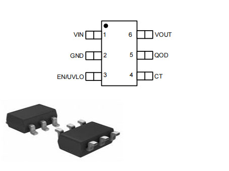
The following figure is TPS22810TDBVRQ1 Pinout.

Pinout


Pin Number Pin Name Description
4 CT Switch slew rate control. Can be left floating
3 EN/UVLO Active high switch control input and UVLO adjustment. Do not leave floating
2 GND Device ground
5 QOD Quick Output Discharge pin. This functionality can be enabled in one of three ways:
• Placing an external resistor between VOUT and QOD
• Tying QOD directly to VOUT and using the internal resistor value (RPD)
• Disabling QOD by leaving pin floating
1 VIN Switch input. Place ceramic bypass capacitor(s) between this pin and GND
6 VOUT Switch output

TPS22810TDBVRQ1 CAD Model

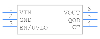
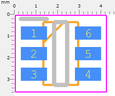
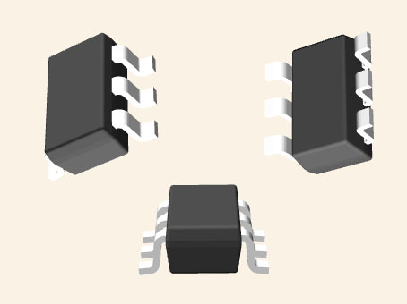
The following figures are TPS22810TDBVRQ1 Symbol, Footprint and 3D Model.

Symbol

Footprint

3D Model

TPS22810TDBVRQ1 Features

• Qualified for Automotive Applications 

• AEC-Q100  Qualified With the Following Results:

– Device Temperature Grade 2: –40°C to +105°C

 Ambient Operating Temperature

– Device HBM ESD Classification Level 2

– Device CDM ESD Classification Level C5

• Integrated Single Channel Load Switch 

• 2-A Maximum Continuous Current 

• Input Voltage: 2.7 V to 18 V

• Absolute Maximum Input Voltage: 20 V

• On-Resistance (RON)

– RON = 79 mΩ (Typical) at  VIN  = 12 V

• Quiescent Current 

– 62 µA (Typical) at  VIN = 12 V

• Shutdown Current

– 500 nA (Typical) at VIN = 12 V

• Thermal Shutdown

•  Undervoltage Lock-Out  (UVLO)

• Adjustable Quick Output Discharge (QOD)

• Configurable Rise Time With CT Pin

•  SOT23 -6 Package

– 2.9-mm × 2.8-mm, 0.95-mm Pitch, 1.45-mm Height (DBV)

Specifications

TPS22810TDBVRQ1 Tech Specifications

Texas Instruments TPS22810TDBVRQ1 technical specifications, attributes, parameters and parts with similar specifications to Texas Instruments TPS22810TDBVRQ1.

Product Attribute Attribute Value
Factory Lead Time6 Weeks
Mounting TypeSurface Mount
Package / CaseSOT-23-6
Surface MountYES
Operating Temperature-40°C~105°C TA
PackagingTape & Reel (TR)
SeriesAutomotive, AEC-Q100
JESD-609 Codee4
Pbfree Codeyes
Part StatusActive
Moisture Sensitivity Level (MSL)2 (1 Year)
Number of Terminations6Terminations
ECCN CodeEAR99
Product Attribute Attribute Value
Terminal FinishNickel/Palladium/Gold (Ni/Pd/Au)
Terminal PositionDUAL
Terminal FormGULL WING
Number of Functions1Function
Terminal Pitch0.95mm
Base Part NumberTPS22810
JESD-30 CodeR-PDSO-G6
Number of Outputs1Output
Output TypeN-Channel
Supply Voltage-Min (Vsup)2.7V
InterfaceOn/Off
Output ConfigurationHigh Side
Voltage - Supply (Vcc/Vdd)2.7V~18V
Product Attribute Attribute Value
Input TypeNon-Inverting
Switch TypeGeneral Purpose
Ratio - Input:Output1:1
Voltage - Load2.7V~18V
Fault ProtectionOver Temperature, UVLO
Rds On (Typ)79m Ω
Built-in ProtectionsTHERMAL; UNDER VOLTAGE
Output Current Flow DirectionSINK
FeaturesLoad Discharge, Slew Rate Controlled
Length2.9mm
RoHS StatusROHS3 Compliant
0 Products View Similar

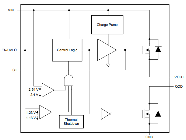
TPS22810TDBVRQ1 Functional Block Diagram

The following figure is TPS22810TDBVRQ1 Functional Block Diagram.

Functional Block Diagram

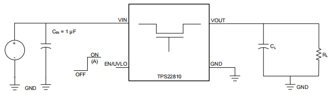
TPS22810TDBVRQ1 Test Circuit

The following is TPS22810TDBVRQ1 Test Circuit.

Test Circuit

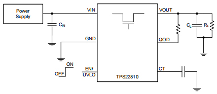
TPS22810TDBVRQ1 Simplified Schematic

The TPS22810TDBVRQ1 Simplified Schematic is shown as follows.

Simplified Schematic

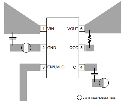
TPS22810TDBVRQ1 Layout

1. To accommodate high current, VIN and VOUT traces must be as short and wide as possible.

2. Ceramic bypass capacitors with low ESR must be used to connect the VIN pin to ground. 1-F ceramic with X5R or X7R dielectric is a standard recommended bypass capacitance. This capacitor should be as close as feasible to the device pins.

Layout

TPS22810TDBVRQ1 Applications

• Automotive Head Unit

• Surround View ECU

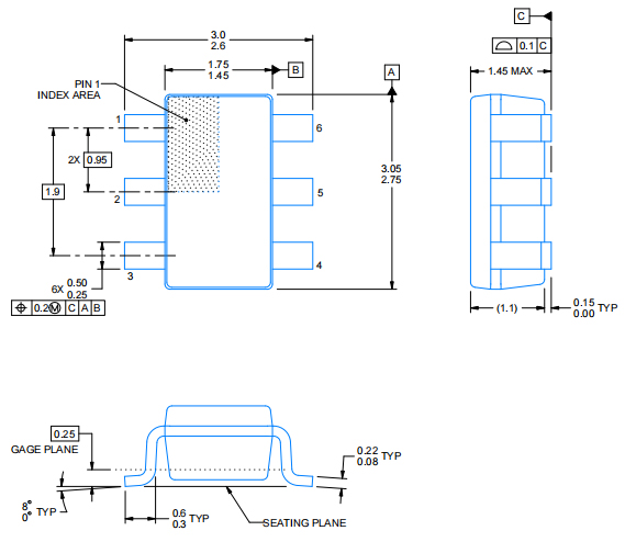
TPS22810TDBVRQ1 Package

The TPS22810TDBVRQ1 Package is shown as follows.

Package

TPS22810TDBVRQ1 Manufacturer

Texas Instruments Incorporated (TI) is an American technology corporation based in Dallas, Texas, that creates and manufactures semiconductors and integrated circuits for electronic designers and manufacturers around the world. Based on sales volume, it is one among the top ten semiconductor businesses in the world. Analog chips and embedded processors, which account for more than 80% of the company's revenue, are the company's main focus. TI also makes calculators, microcontrollers, and multi-core processors, as well as TI digital light processing technologies and education technology.


Frequently Asked Questions

What is a single-channel load switch with adjustable rising time and rapid output discharge?
TPS22810TDBVRQ1.
What feature protects the TPS22810TDBVRQ1 from high junction temperatures?
Thermal shutdown.
What is used in the TPS22810TDBVRQ1?
N-channel MOSFET.
What is the maximum current of the TPS22810TDBVRQ1?
2 A.
What minimizes inrush current generated by large bulk load capacitances?
Programmable rise time.
What turns off the device if the VIN voltage falls below a certain threshold?
Undervoltage lock-out.
What controls the devices fall time?
The programmable QOD pin.
What is the TPS22810TDBVRQ1 offered in?
Solder connections.
What is the temperature range of the TPS22810TDBVRQ1?
–40°C to +105°C.
FAQ
What is a single-channel load switch with adjustable rising time and rapid output discharge?
TPS22810TDBVRQ1.
What feature protects the TPS22810TDBVRQ1 from high junction temperatures?
Thermal shutdown.
What is used in the TPS22810TDBVRQ1?
N-channel MOSFET.
What is the maximum current of the TPS22810TDBVRQ1?
2 A.
What minimizes inrush current generated by large bulk load capacitances?
Programmable rise time.
What turns off the device if the VIN voltage falls below a certain threshold?
Undervoltage lock-out.
What controls the devices fall time?
The programmable QOD pin.
What is the TPS22810TDBVRQ1 offered in?
Solder connections.
What is the temperature range of the TPS22810TDBVRQ1?
–40°C to +105°C.

TAGS

Share