Episode 10: Load Switches Ahead
The TPS22918-Q1 is a 6-pin SOT-23 load switch with a 5.5-V, 2-A rating. This article mainly introduces Schematic, Pinout, Datasheet and other detailed information about Texas Instruments TPS22918TDBVRQ1.

The TPS22918-Q1 is a 6-pin SOT-23 load switch with a 5.5-V, 2-A rating. This article mainly introduces Schematic, Pinout, Datasheet and other detailed information about Texas Instruments TPS22918TDBVRQ1.
453
Mar 30, 2022
Perry Jim
Episode 10: Load Switches Ahead
The TPS22918-Q1 is a 6-pin SOT-23 load switch with a 5.5-V, 2-A rating. This article mainly introduces Schematic, Pinout, Datasheet and other detailed information about Texas Instruments TPS22918TDBVRQ1.
TPS22918TDBVRQ1
The TPS22918TDBVRQ1 is a 6-pin SOT-23 load switch with a 5.5-V, 2-A rating. The device uses a low resistance N-channel MOSFET to reduce voltage drop for low voltage and high current rails, lowering the drop out voltage through the device.
The device includes a slew rate that may be adjusted to help decrease or eliminate power supply droop caused by excessive inrush currents. The device also has a QOD pin, which can be used to set the VOUT discharge rate once the switch is turned off. The device features very low leakage currents during shutdown, which reduces unwanted leakages for downstream modules during standby. External components are eliminated due to the integrated control logic, driver, charge pump, and output discharge FET, resulting in a smaller solution and lower bill of materials (BOM) count.
The device's adjustable rise time minimizes inrush current induced by large bulk load capacitances, lowering or eliminating power supply droop. The TPS22918TDBVRQ1 has a customizable rapid output discharge (QOD) pin that adjusts the device's fall time, allowing for design flexibility in terms of power down and sequencing.
The TPS22918TDBVRQ1 is packaged in a tiny, leaded SOT-23 package (DBV) that allows solder joints to be visually inspected. The gadget is designed to operate in a temperature range of –40°C to +105°C in free air.
The following figure is TPS22918TDBVRQ1 Pinout.
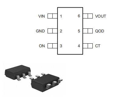
Pinout
| Pin Number | Pin Name | Description |
| 1 | VIN | Switch input. Place ceramic bypass capacitor(s) between this pin and GND. |
| 2 | GND | Device ground |
| 3 | ON | Active high switch control input. Do not leave floating |
| 4 | CT | Switch slew rate control. Can be left floating. |
| 5 | QOD | Quick Output Discharge pin. This functionality can be enabled in one of three ways • Placing an external resistor between VOUT and QOD • Tying QOD directly to VOUT and using the internal resistor value (RPD) • Disabling QOD by leaving pin disconnected |
| 6 | VOUT | Switch output |
The followings are TPS22918TDBVRQ1 Symbol, Footprint and 3D Model.

Symbol
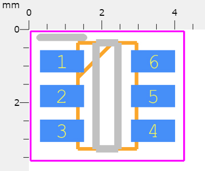
Footprint
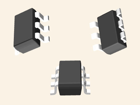
3D Model
• AEC-Q100 Qualified
• Integrated single-channel load switch
• Qualified for automotive applications:
– Device Temperature Grade 2: –40°C to +105°C ambient operating temperature range
• Functional safety capable
– Documentation available to aid functional safety system design
• Input voltage range: 1 V to 5.5 V
• Low On-Resistance (RON) – RON = 52 mΩ (typical) at VIN = 5 V – RON = 53 mΩ (typical) at VIN = 3.3 V
• 2-A Maximum continuous switch current
• Low quiescent current
– 8.3 µA (typical) at VIN = 3.3 V • Low-control input-threshold enables use of 1 V or higher GPIO
• Configurable Quick-Output Discharge (QOD)
• Configurable rise time with CT pin
• Small SOT23-6 package (DBV)
– 2.9 mm × 2.8 mm, 0.95-mm Pitch, 1.45-mm height (with leads)
• ESD Performance tested per AEC Q100
– ±2-kV HBM and ±750-V CDM
Texas Instruments TPS22918TDBVRQ1 technical specifications, attributes, parameters and parts with similar specifications to Texas Instruments TPS22918TDBVRQ1.
| Product Attribute | Attribute Value | |
|---|---|---|
| Lifecycle Status | ACTIVE (Last Updated: 5 days ago) | |
| Factory Lead Time | 6 Weeks | |
| Mounting Type | Surface Mount | |
| Package / Case | SOT-23-6 | |
| Surface Mount | YES | |
| Number of Pins | 6Pins | |
| Operating Temperature | -40°C~105°C TA | |
| Packaging | Tape & Reel (TR) | |
| Series | Automotive, AEC-Q100 | |
| JESD-609 Code | e3 | |
| Pbfree Code | yes | |
| Part Status | Active | |
| Moisture Sensitivity Level (MSL) | 3 (168 Hours) | |
| Number of Terminations | 6Terminations |
| Product Attribute | Attribute Value | |
|---|---|---|
| ECCN Code | EAR99 | |
| Terminal Finish | Matte Tin (Sn) | |
| Voltage - Supply | Not Required | |
| Terminal Position | DUAL | |
| Terminal Form | GULL WING | |
| Number of Functions | 1Function | |
| Terminal Pitch | 0.95mm | |
| Base Part Number | TPS22918 | |
| Number of Outputs | 1Output | |
| Output Type | N-Channel | |
| Interface | On/Off | |
| Output Configuration | High Side | |
| Input Type | Non-Inverting | |
| Switch Type | General Purpose |
| Product Attribute | Attribute Value | |
|---|---|---|
| Ratio - Input:Output | 1:1 | |
| Voltage - Load | 1V~5.5V | |
| Rds On (Typ) | 52m Ω | |
| Built-in Protections | TRANSIENT | |
| Output Current Flow Direction | SINK | |
| Features | Load Discharge, Slew Rate Controlled | |
| Height | 1.45mm | |
| Length | 2.9mm | |
| Width | 1.6mm | |
| Thickness | 1.2mm | |
| RoHS Status | ROHS3 Compliant | |
| Lead Free | Lead Free |
The following figure is TPS22918TDBVRQ1 Functional Block Diagram.
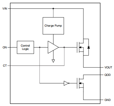
Functional Block Diagram
The following shows TPS22918TDBVRQ1 Test Circuit.
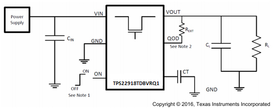
Test Circuit
(1) The control signal's rise and fall times are 100 nanoseconds.
(2) Turnoff and fall times are influenced by the load's time constant. When the switch is deactivated on the TPS22918TDBVRQ1, the internal pull-down resistance RPD is enabled. (RQOD || RL) CL is the time constant, where RQOD equals RPD + REXT.
This typical application demonstrates how the TPS22918TDBVRQ1 can be used to power downstream modules.
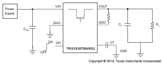
Typical Application Schematic
• To accommodate high current, VIN and VOUT traces must be as short and wide as feasible.
• Ceramic bypass capacitors with low ESR must be used to connect the VIN pin to ground. 1F ceramic with X5R or X7R dielectric is a standard recommended bypass capacitance. This capacitor should be as close as feasible to the device pins.
• Ceramic bypass capacitors with low ESR must be used to connect the VOUT pin to ground. The suggested bypass capacitance is one-tenth of the VIN bypass capacitor with dielectric ratings of X5R or X7R.
This capacitor should be as close as feasible to the device pins.
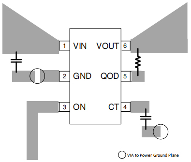
Layout
• Automotive electronics
• Infotainment
• Cluster
• ADAS (Advanced Driver Assistance Systems)
The following figure is TPS22918TDBVRQ1 Package.
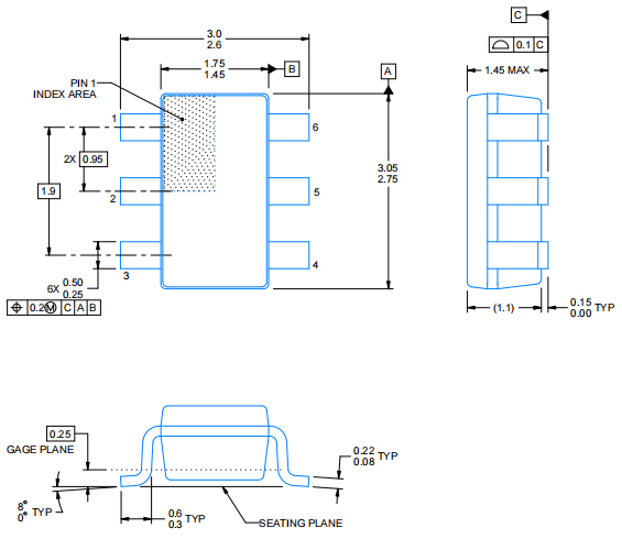
Package
Texas Instruments Incorporated (TI) is an American technology corporation based in Dallas, Texas, that creates and manufactures semiconductors and integrated circuits for electronic designers and manufacturers around the world. Based on sales volume, it is one of the top ten semiconductor businesses in the world. Analog chips and embedded processors, which account for more than 80% of the company's revenue, are the company's main focus. TI also makes calculators, microcontrollers, and multi-core processors, as well as TI digital light processing technologies and education technology.
TAGS
Comments