ATTENTION: Due to increased demand and order volume, processing time may take an additional 1-3 business days.
HomeCommunitySubjectTPS22919DCKR Load Switch: Features, Pinout, and Datasheet

TPS22919DCKR Load Switch: Features, Pinout, and Datasheet

5.5V, 1.5A, 90m? self-protected load switch with controlled rise time 6-SC70 -40 to 105 The TPS22919 is a 6-pin SOT-23 device with a 5.5-V, 1.5-A load switch. This article mainly introduces Features, Pinout, Datasheet and other detailed information about Texas Instruments TPS22919DCKR.

270

Mar 31, 2022

Lance Lindsay

What is a load switch


5.5V, 1.5A, 90m? self-protected load switch with controlled rise time 6-SC70 -40 to 105

The TPS22919 is a 6-pin SOT-23 device with a 5.5-V, 1.5-A load switch. This article mainly introduces Features, Pinout, Datasheet and other detailed information about Texas Instruments TPS22919DCKR.


TPS22919DCKR

101693In Stock
Min.: 1 Mult.: 1
Quantity Unit Price Ext. Price
1+ $2.2$2.2
10+ $1.49$14.9
25+ $1.316$32.9
100+ $1.122$112.2
250+ $1.03$257.5
500+ $0.9744$487.2
1000+ $0.9288$928.8
Unit Price:$0.9288
Subtotal: $0.93
Looking for a better price? Want a lower wholesale price? Please send an RFQ, and we will respond immediately.
Quick Links

TPS22919DCKR Description

The TPS22919DCKR is a 6-pin SOT-23 device with a 5.5-V, 1.5-A load switch. The device uses a low resistance N-channel MOSFET to reduce voltage drop for low voltage and high current rails, lowering the drop-out voltage across the device.

A digital input capable of directly connecting with low-voltage control signals controls the switch ON state. A Smart Pull Down is utilized to keep the ON pin from floating until the system sequence is complete when power is initially delivered. The Smart Pull Down will be disconnected once the pin is intentionally driven high (>VIH) to prevent unnecessary power loss.

The TPS22919DCKR load switch is also self-protected, which means it will protect itself in the event of a short circuit on the device's output. It also supports thermal shutdown to prevent overheating damage.

TPS22919DCKR is offered in a standard SC-70 package with a junction temperature range of –40°C to 125°C for operation.

TPS22919DCKR Pinout

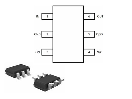
The following figure is TPS22919DCKR Pinout.

Pinout


Pin Number Pin Name Description
1 IN Switch input.
2 GND Device ground.
3 ON Active high switch control input. Do not leave floating.
4 NC No connect pin, leave floating.
5 QOD Quick Output Discharge pin. This functionality can be enabled in one of three ways.
• Placing an external resistor between VOUT and QOD
• Tying QOD directly to VOUT and using the internal resistor value (RPD)
• Disabling QOD by leaving pin floating
6 VOUT Switch output.

TPS22919DCKR CAD Model

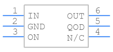
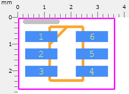
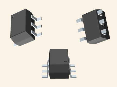
The TPS22919DCKR CAD Model is shown as follows.

Symbol

Footprint

3D Model

TPS22919DCKR Features

• Input operating voltage range (VIN): 1.6 V to 5.5 V

• Maximum continuous current (IMAX): 1.5 A • On-Resistance (RON):

– 5-V VIN: 89 mΩ (typical)

– 3.6-V VIN: 90 mΩ (typical)

– 1.8-V VIN: 105 mΩ (typical)

• Output short protection (ISC): 3 A (typical)

• Low power consumption:

– ON state (IQ): 8 µA (typical)

– OFF state (ISD): 2 nA (typical)

• Smart ON pin pull down (RPD):

– ON ≥ VIH (ION): 100 nA (maximum)

– ON ≤ VIL (RPD): 530 kΩ (typical)

• Slow Turn ON timing to limit inrush current (tON):

– 5.0 V Turn ON time (tON): 1.95 ms at 3.2 mV/μs

– 3.6 V Turn ON time (tON): 1.75 ms at 2.7 mV/μs

– 1.8 V Turn ON time (tON): 1.5 ms at 1.8 mV/μs

• Adjustable output discharge and fall time:

– Internal QOD resistance = 24 Ω (typical)

Specifications

TPS22919DCKR Tech Specifications

Texas Instruments TPS22919DCKR technical specifications, attributes, parameters and parts with similar specifications to Texas Instruments TPS22919DCKR.

Product Attribute Attribute Value
Factory Lead Time6 Weeks
Mounting TypeSurface Mount
Package / Case6-TSSOP, SC-88, SOT-363
Surface MountYES
Operating Temperature-40°C~125°C TA
PackagingTape & Reel (TR)
JESD-609 Codee3
Pbfree Codeyes
Part StatusActive
Moisture Sensitivity Level (MSL)1 (Unlimited)
Number of Terminations6Terminations
Terminal FinishMatte Tin (Sn)
Product Attribute Attribute Value
Terminal PositionDUAL
Terminal FormGULL WING
Number of Functions1Function
Terminal Pitch0.65mm
Base Part NumberTPS22919
JESD-30 CodeR-PDSO-G6
Number of Outputs1Output
Output TypeN-Channel
InterfaceOn/Off
Output ConfigurationHigh Side
Voltage - Supply (Vcc/Vdd)Not Required
Input TypeNon-Inverting
Product Attribute Attribute Value
Switch TypeGeneral Purpose
Ratio - Input:Output1:1
Voltage - Load1.6V~5.5V
Fault ProtectionShort Circuit
Output Peak Current Limit-Nom3A
Rds On (Typ)89m Ω
Built-in ProtectionsTRANSIENT; OVER CURRENT; THERMAL
Output Current Flow DirectionSINK
FeaturesLoad Discharge, Slew Rate Controlled
Length2mm
RoHS StatusROHS3 Compliant
0 Products View Similar

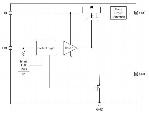
TPS22919DCKR Functional Block Diagram

The following figure is TPS22919DCKR Functional Block Diagram.

Functional Block Diagram

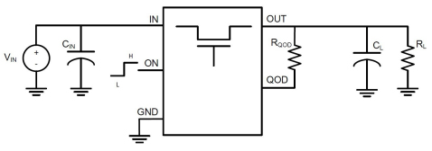
TPS22919DCKR Simplified Schematic

The following figure is TPS22919DCKR Simplified Schematic.

Simplified Schematic

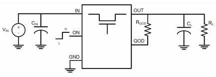
TPS22919DCKR Test Circuit

The TPS22919DCKR Test Circuit is shown as follows.

Test Circuit

(1) The control signal's rise and fall times are 100 nanoseconds.

(2) The time constant at the load affects the turn-off and fall times. When the switch is deactivated on the TPS22919 devices, the internal pull-down resistance QOD is enabled. (RQOD + RPD,QOD || RL) *CL is the time constant.

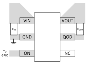
TPS22919DCKR Layout

All traces must be as brief as possible for optimal performance. In order to reduce the impacts of parasitic trace inductances on normal operation, the input and output capacitors must be located close to the device. The parasitic electrical effects are reduced by using large traces for VIN, VOUT, and GND.

Layout

TPS22919DCKR Applications

• Personal electronics

• Set-top box

• HDTV

• Multi function printer

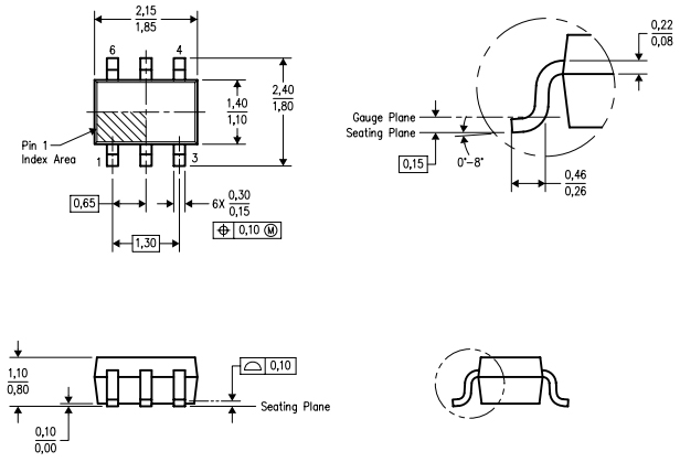
TPS22919DCKR Package

The TPS22919DCKR Package is shown as follows.

Package

TPS22919DCKR Manufacturer

Texas Instruments (TI), a multinational semiconductor business with operations in 35 countries, is first and foremost a reflection of its employees. We are problem-solvers cooperating to transform the world via technology, from the TIer who introduced the first functional integrated circuit in 1958 to the more than 30,000 TIers throughout the world today who develop, build, and distribute analog and embedded processor chips.

Frequently Asked Questions

What is the TPS22919DCKR?
5.5 V, 1.5 A, 90-mΩ Self-Protected Load Switch with Controlled Rise Time.
What does the TPS22919DCKR use to reduce voltage drop?
Low resistance N-channel MOSFET.
What does a digital input do to the TPS22919DCKR?
A digital input capable of directly connecting with low-voltage control signals controls the switch ON state.
What is used to keep the ON pin from floating until the system sequence is complete when power is initially delivered?
A Smart Pull Down.
What is the TPS22919DCKR load switch?
Self-protected.
What does the TPS22919DCKR support to prevent overheating damage?
Thermal shutdown.
What is the junction temperature range of the TPS22919DCKR?
–40°C to 125°C for operation.
FAQ
What is the TPS22919DCKR?
5.5 V, 1.5 A, 90-mΩ Self-Protected Load Switch with Controlled Rise Time.
What does the TPS22919DCKR use to reduce voltage drop?
Low resistance N-channel MOSFET.
What does a digital input do to the TPS22919DCKR?
A digital input capable of directly connecting with low-voltage control signals controls the switch ON state.
What is used to keep the ON pin from floating until the system sequence is complete when power is initially delivered?
A Smart Pull Down.
What is the TPS22919DCKR load switch?
Self-protected.
What does the TPS22919DCKR support to prevent overheating damage?
Thermal shutdown.
What is the junction temperature range of the TPS22919DCKR?
–40°C to 125°C for operation.

TAGS

Share