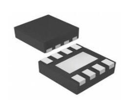
The TPS22965 is a single channel load switch. This article mainly covers its pinout, datasheet, typical application circuit and more about TPS22965.

The TPS22965 is a single channel load switch. This article mainly covers its pinout, datasheet, typical application circuit and more about TPS22965.
461
Mar 1, 2022
Mag Caroline
The TPS22965 is a single channel load switch. This article mainly covers its pinout, datasheet, typical application circuit and more about TPS22965.
TPS22965DSGR
| Quantity | Unit Price | Ext. Price |
|---|---|---|
| 1+ | $8.7 | $8.7 |
| 10+ | $6.2 | $62 |
| 25+ | $5.576 | $139.4 |
| 100+ | $4.898 | $489.8 |
| 250+ | $4.5732 | $1143.3 |
| 500+ | $4.3776 | $2188.8 |
| 1000+ | $4.2228 | $4222.8 |
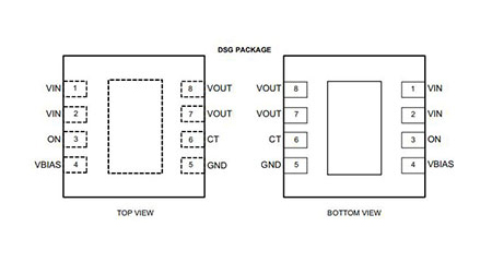
TPS22965 Pinout
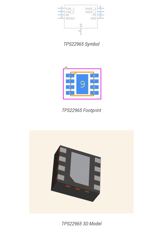
The TPS22965 is a single channel load switch that provides configurable rise time to minimize inrush current. The device contains an N-channel MOSFET that can operate over an input voltage range of 0.8 V to 5.7 V and can support a maximum continuous current of 6 A. The switch is controlled by an on/off input (ON), which is capable of interfacing directly with low-voltage control signals. In the TPS22965, a 225-0 on-chip load resistor is added for quick output discharge when the switch is turned off The TPS22965 is available in a small, space-saving 2.00 mm x 2.00 mm 8-pin SON package (DSG) with an integrated thermal pad allowing for high power dissipation. The device is characterized for operation over the free-air temperature range of - -40 °C to 105 °C.
Integrated Single Channel Load Switch
Input Voltage Range: 0.7 V to 5 .7 V
RON Resistance
RON = 14 mΩ at VIN = 5 V (VBIAS = 5 V)
5-A Maximum Continuous Switch Current
Adjustable Undervoltage Lockout Threshold (UVLO)
Adjustable Voltage Supervisor with Power Good (PG) Indicator
Adjustable Output Slew Rate Control
Enhanced Quick Output Discharge Remains Active after Power is Removed (TPS22954 Only)
15 Ω (Typ) Discharges 100 µF Within 10 ms
Reverse Current Blocking when Disabled (TPS22953 Only)
Automatic Restart after Supervisor Fault Detection When Enabled
Thermal Shutdown
Low Quiescent Current ≤ 50 µA
SON 10 -pin Package with Thermal Pad
ESD Performance Tested Per JESD 22
2-kV HBM and 750 -V CDM
●UltrabookTM
●Notebooks/Netbooks
●Tablet PC
●Consumer Electronics
●Set-top Boxes/Residential Gateways
●Telecom Systems
●Solid State Drives (SSDs)
The TPS22965 device is a single channel, 6-A load switch in an 8-pin SON package. To reduce the voltage drop in high current rails, the device implements an ultra-low resistance N-channel MOSFET. The device has a programmable slew rate for applications that require specific rise-time. The device has a very low leakage current during off state. This prevents downstream circuits from pulling high standby current from the supply. Integrated control logic, driver, power supply, and output discharge FETeliminates the need for any external components, which reduces solution size and bill of materials (BOM) count. The functional block diagram is shown below.
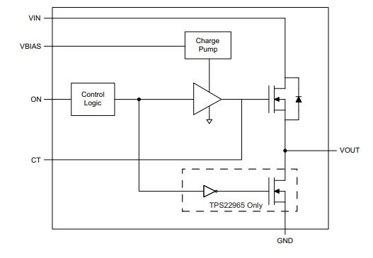
TPS22965 Functional Block Diagram
This application demonstrates how the TPS22965 can be used to power downstream modules.
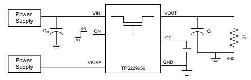
TPS22965-Powering a Downstream Module

Texas Instruments TPS22965DSGR technical specifications, attributes, parameters and parts with similar specifications to Texas Instruments TPS22965DSGR.
| Product Attribute | Attribute Value | |
|---|---|---|
| Lifecycle Status | ACTIVE (Last Updated: 5 days ago) | |
| Factory Lead Time | 6 Weeks | |
| Contact Plating | Gold | |
| Mount | Surface Mount | |
| Mounting Type | Surface Mount | |
| Package / Case | 8-WFDFN Exposed Pad | |
| Number of Pins | 8Pins | |
| Turn Off Delay Time | 80 μs | |
| Operating Temperature | -40°C~105°C TA | |
| Packaging | Tape & Reel (TR) | |
| JESD-609 Code | e4 | |
| Pbfree Code | yes | |
| Part Status | Active | |
| Moisture Sensitivity Level (MSL) | 2 (1 Year) | |
| Number of Terminations | 8Terminations | |
| ECCN Code | EAR99 | |
| Resistance | 25mOhm | |
| Voltage - Supply | 0.8V~5.7V |
| Product Attribute | Attribute Value | |
|---|---|---|
| Terminal Position | DUAL | |
| Peak Reflow Temperature (Cel) | 260 | |
| Number of Functions | 1Function | |
| Supply Voltage | 5V | |
| Terminal Pitch | 0.5mm | |
| Base Part Number | TPS22965 | |
| Number of Outputs | 1Output | |
| Output Type | N-Channel | |
| Max Output Current | 6A | |
| Interface | On/Off | |
| Output Configuration | High Side | |
| Current - Output | 6A | |
| Quiescent Current | 50μA | |
| Input Type | Non-Inverting | |
| Turn On Delay Time | 2.2 ms | |
| Switch Type | General Purpose | |
| Nominal Input Voltage | 5.7V | |
| Output Polarity | TRUE |
| Product Attribute | Attribute Value | |
|---|---|---|
| Ratio - Input:Output | 1:1 | |
| Input Characteristics | STANDARD | |
| Voltage - Load | 2.5V~5.7V | |
| Driver Number of Bits | 1Bit | |
| Rds On (Typ) | 16m Ω | |
| Max Junction Temperature (Tj) | 125°C | |
| Voltage - Supply (Min) | 2.5V | |
| Built-in Protections | TRANSIENT | |
| Features | Load Discharge, Slew Rate Controlled | |
| On-State Resistance | 25mOhm | |
| Height | 800μm | |
| Length | 2mm | |
| Width | 2mm | |
| Thickness | 750μm | |
| REACH SVHC | No SVHC | |
| Radiation Hardening | No | |
| RoHS Status | ROHS3 Compliant | |
| Lead Free | Lead Free |
TAGS
Comments