ATTENTION: Due to increased demand and order volume, processing time may take an additional 1-3 business days.
HomeCommunitySubjectTPS22965NQWDSGRQ1 On-Resistance Load Switch: Circuit, Pinout, and Datasheet

TPS22965NQWDSGRQ1 On-Resistance Load Switch: Circuit, Pinout, and Datasheet

IC LOAD SWITCH 6A 8WSON The TPS22965NQWDSGRQ1 is a single-channel load switch with a controlled turn-on that is compact and ultralow RON. This article mainly introduces Circuit, Pinout, Datasheet and other detailed information about Texas Instruments TPS22965NQWDSGRQ1.

95

Apr 6, 2022

Hilda Malory

TI New Product Update: Load Switches


IC LOAD SWITCH 6A 8WSON

The TPS22965NQWDSGRQ1 is a single-channel load switch with a controlled turn-on that is compact and ultralow RON. This article mainly introduces Circuit, Pinout, Datasheet and other detailed information about Texas Instruments TPS22965NQWDSGRQ1.

TPS22965NQWDSGRQ1

903In Stock
Min.: 1 Mult.: 1
Price not displayed? Not available to buy online? Please send an RFQ, and we will respond immediately.
Quick Links

TPS22965NQWDSGRQ1 Description

The TPS22965NQWDSGRQ1 is a single-channel load switch with a controlled turn-on that is compact and ultralow RON. An N-channel MOSFET  is included in the device, which can function between 0.8 and 5.5 V and sustain a maximum continuous current of 4A. The rising time of VOUT can be adjusted to reduce the inrush current. When the switch is switched off, the TPS22965NQWDSGRQ1 device has a 225-ohm on-chip load resistor for rapid output discharge.

The TPS22965NQWDSGRQ1 device comes in a 2-mm * 2-mm 8-pin WSON package (DSG0008A) with an integrated thermal pad for high power dissipation. The TPS22965NQWDSGRQ1 device is designed to operate in a temperature range of –40°C to 105°C in free air.

TPS22965NQWDSGRQ1 Pinout

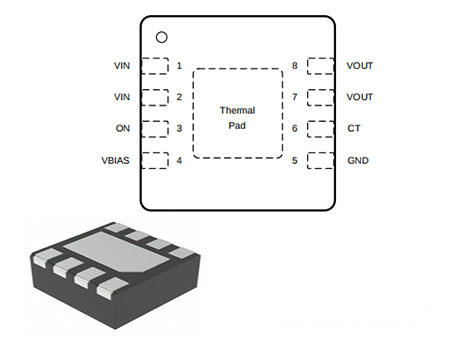
The following figure is TPS22965NQWDSGRQ1 Pinout.

Pinout


Pin Number Pin Name Description
1,2 VIN Switch input. Input bypass capacitor recommended for minimizing VIN dip. Must be connected to
Pin 1 and Pin 2.
3 ON Active high switch control input. Do not leave floating
4 VBIAS Bias voltage. Power supply to the device. Recommended voltage range for this pin is 2.5 V to 5.5 V.
5 GND Device ground
6 CT Switch slew rate control. Can be left floating.
7,8 VOUT Switch output
  Thermal pad Thermal pad (exposed center pad) to alleviate thermal stress. Tie to GND

TPS22965NQWDSGRQ1 CAD Model

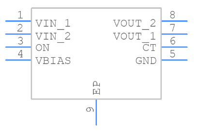
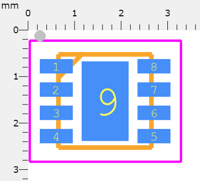
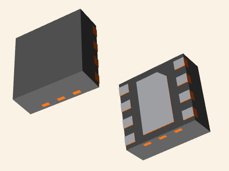
The followings are TPS22965NQWDSGRQ1 Symbol, Footprint and 3D Model.

Symbol

Footprint

3D Model

TPS22965NQWDSGRQ1 Features

• Qualified for Automotive Applications

– AEC-Q100 Qualified

– Device Temperature Grade 2: –40°C to +105°C

– Device HBM ESD Classification Level 3A

– Device CDM ESD Classification Level C6

• Functional safety capable

– Documentation available to aid functional safety system design

• Integrated Single Channel Load Switch

• Input Voltage Range: 0.8 V to 5.5 V • Ultra-Low On Resistance (RON) – RON = 16 mΩ at  VIN  = 5 V (VBIAS = 5 V)

– RON = 16 mΩ at VIN = 3.6 V (VBIAS = 5 V)

– RON = 16 mΩ at VIN = 1.8 V (VBIAS = 5 V)

• 4-A Maximum Continuous Switch Current

• Low Quiescent Current (50 µA)

• Low Control Input Threshold Enables Use of 1.2-, 1.8-, 2.5- and 3.3-V Logic

• Configurable  Rise Time 

• Quick Output Discharge (QOD)

• WSON 8-pin Package with Thermal Pad

Specifications

TPS22965NQWDSGRQ1 Tech Specifications

Texas Instruments TPS22965NQWDSGRQ1 technical specifications, attributes, parameters and parts with similar specifications to Texas Instruments TPS22965NQWDSGRQ1.

Product Attribute Attribute Value
Lifecycle StatusACTIVE (Last Updated: 4 days ago)
Factory Lead Time6 Weeks
Mounting TypeSurface Mount
Package / Case8-WFDFN Exposed Pad
Surface MountYES
Number of Pins8Pins
Operating Temperature-40°C~125°C TA
PackagingTape & Reel (TR)
SeriesAutomotive, AEC-Q100
JESD-609 Codee3
Pbfree Codeyes
Part StatusActive
Moisture Sensitivity Level (MSL)2 (1 Year)
Number of Terminations8Terminations
ECCN CodeEAR99
Product Attribute Attribute Value
Terminal FinishMatte Tin (Sn)
Terminal PositionDUAL
Terminal FormNO LEAD
Number of Functions1Function
Supply Voltage5V
Terminal Pitch0.5mm
Base Part NumberTPS22965
Number of Outputs1Output
Output TypeN-Channel
Max Output Current4A
Supply Voltage-Max (Vsup)5.5V
Supply Voltage-Min (Vsup)2.5V
InterfaceOn/Off
Output ConfigurationHigh Side
Voltage - Supply (Vcc/Vdd)0.8V~5.5V
Product Attribute Attribute Value
Input TypeNon-Inverting
Switch TypeGeneral Purpose
Ratio - Input:Output1:1
Voltage - Load2.5V~5.5V
Output Peak Current Limit-Nom1A
Rds On (Typ)16m Ω
Built-in ProtectionsTRANSIENT
Output Current Flow DirectionSINK
FeaturesSlew Rate Controlled
Height800μm
Length2mm
Width2mm
Thickness750μm
RoHS StatusROHS3 Compliant
Lead FreeLead Free
0 Products View Similar

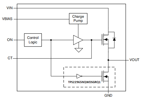
TPS22965NQWDSGRQ1 Functional Block Diagram

The TPS22965NQWDSGRQ1 Functional Block Diagram is shown as follows.

Functional Block Diagram

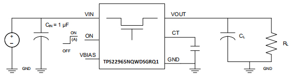
TPS22965NQWDSGRQ1 Test Circuit

The TPS22965NQWDSGRQ1 Test Circuit is shown as follows.

Test Circuit

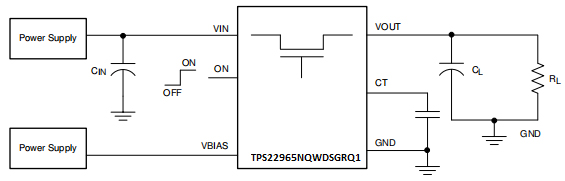
TPS22965NQWDSGRQ1 Typical Application

This application demonstrates how the TPS22965NQWDSGRQ1 can be used to power downstream modules.

Schematic for Powering a Downstream Module

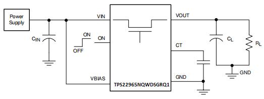
TPS22965NQWDSGRQ1 Simplified Schematic

The following shows the TPS22965NQWDSGRQ1 Simplified Schematic.

Simplified Schematic

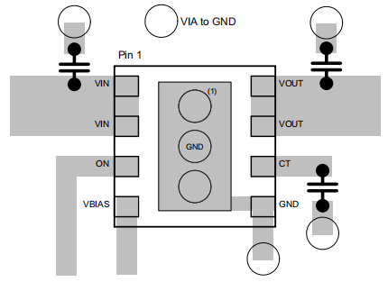
TPS22965NQWDSGRQ1 Layout

All traces must be as brief as possible for optimal performance. In order to reduce the impacts of parasitic trace inductances on normal operation, the input and output capacitors must be located close to the device. The use of large traces for VIN, VOUT, and GND reduces parasitic electrical effects while also lowering case-to-ambient thermal impedance. To avoid parasitic capacitance, the CT trace must be as short as feasible.

Layout

TPS22965NQWDSGRQ1 Alternatives

Part Number Description Manufacturer
TPS22965NQWDSGTQ1DRIVERS AND INTERFACES 1-ch, 5.7-V, 4-A, 16-mΩ automotive load switch with adj. rise time and output discharge 8-WSON -40 to 125 Texas Instruments

TPS22965NQWDSGRQ1 Applications

• Automotive Electronics

• Infotainment

• ADAS (Advanced Driver Assistance Systems)


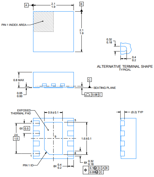
TPS22965NQWDSGRQ1 Package

The TPS22965NQWDSGRQ1 Package is shown as follows.

Package

TPS22965NQWDSGRQ1 Manufacturer

Texas Instruments Incorporated (TI) is an American technology corporation based in Dallas, Texas, that creates and manufactures semiconductors and integrated circuits for electronic designers and manufacturers around the world. Based on sales volume, it is one of the top ten semiconductor businesses in the world. Analog chips and embedded processors, which account for more than 80% of the company's revenue, are the company's main focus. TI also makes calculators, microcontrollers, and multi-core processors, as well as TI digital light processing technologies and education technology.

Frequently Asked Questions

What is the controlled turn-on of the TPS22965NQWDSGRQ1?
Compact and ultralow RON.
What is included in the TPS22965NQWDSGRQ1?
N-channel MOSFET.
How can the rising time of VOUT be adjusted?
Reduce the inrush current.
What is the on-chip load resistor on the TPS22965NQWDSGRQ1 device?
225-ohm.
What type of WSON package does the TPS22965NQWDSGRQ1 come in?
2-mm * 2-mm 8-pin.
What temperature range is the TPS22965NQWDSGRQ1 device designed to operate in?
–40°C to 105°C in free air.
FAQ
What is the controlled turn-on of the TPS22965NQWDSGRQ1?
Compact and ultralow RON.
What is included in the TPS22965NQWDSGRQ1?
N-channel MOSFET.
How can the rising time of VOUT be adjusted?
Reduce the inrush current.
What is the on-chip load resistor on the TPS22965NQWDSGRQ1 device?
225-ohm.
What type of WSON package does the TPS22965NQWDSGRQ1 come in?
2-mm * 2-mm 8-pin.
What temperature range is the TPS22965NQWDSGRQ1 device designed to operate in?
–40°C to 105°C in free air.

TAGS

Share