ATTENTION: Due to increased demand and order volume, processing time may take an additional 1-3 business days.
HomeCommunitySubjectTPS2553DBVR Power-Distribution Switch: Layout, Pinout, and Datasheet

TPS2553DBVR Power-Distribution Switch: Layout, Pinout, and Datasheet

The TPS2553DBVR power-distribution switch provides up to 1.5 A of continuous load current and is designed for situations requiring precision current limiting or heavy capacitive loads and short circuits. This article mainly introduces Layout, Pinout, Datasheet and other detailed information about Texas Instruments TPS2553DBVR.
165

Mar 9, 2022

Bernie Yale

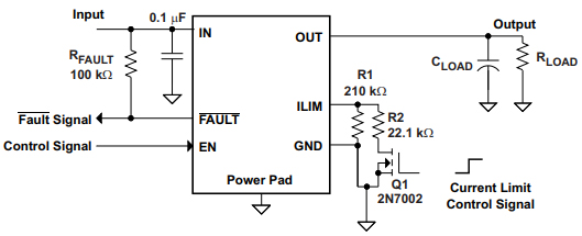
Active Current Limiting Circuit Schematic


The TPS2553DBVR power-distribution switch provides up to 1.5 A of continuous load current and is designed for situations requiring precision current limiting or heavy capacitive loads and short circuits. This article mainly introduces Layout, Pinout, Datasheet and other detailed information about Texas Instruments TPS2553DBVR.
TPS2553DBVR

281In Stock
Min.: 1 Mult.: 1
Quantity Unit Price Ext. Price
1+ $10.9$10.9
10+ $7.86$78.6
25+ $7.096$177.4
100+ $6.258$625.8
250+ $5.8584$1464.6
500+ $5.6178$2808.9
1000+ $5.4774$5477.4
Unit Price:$5.4774
Subtotal: $5.48
Looking for a better price? Want a lower wholesale price? Please send an RFQ, and we will respond immediately.
Quick Links

TPS2553DBVR Description

The TPS2553DBVR power-distribution switch provides up to 1.5 A of continuous load current and is designed for situations requiring precision current limiting or heavy capacitive loads and short circuits. Through an external resistor, these devices provide a configurable current-limit threshold between 75 mA and 1.7 A (typical). At the higher current-limit levels, current-limit accuracy of up to 6% can be reached. To reduce current surges during turnon and turnoff, the rise and fall times of the power switch are managed.

When the output load exceeds the current-limit threshold, the TPS2553DBVR device uses a constant-current mode to limit the output current to a safe level. To protect devices on the input side of the switch, an inbuilt reverse-voltage comparator disables the power switch when the output voltage is driven higher than the input voltage. During overcurrent and reverse-voltage circumstances, the FAULT output asserts low.

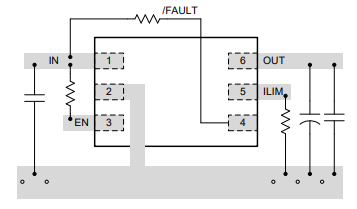
TPS2553DBVR Pinout

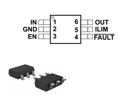
he following figure is TPS2553DBVR Pinout.

Pinout


Pin Number Pin Name Description
3 EN Enable input, logic low turns on power switch
4 FAULT Active-low open-drain output, asserted during overcurrent, overtemperature, or reverse-voltage conditions.
2 GND Ground connection; connect externally to PowerPAD
5 ILIM External resistor used to set current-limit threshold; recommended 15 kΩ ≤ RILIM ≤ 232 kΩ.
1 IN Input voltage; connect a 0.1 μF or greater ceramic capacitor from IN to GND as close to the IC as possible.
6 OUT Power-switch output

TPS2553DBVR CAD Model

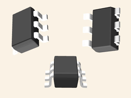
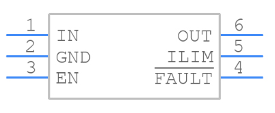
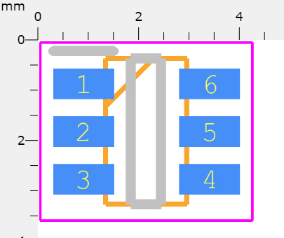
The followings are TPS2553DBVR Symbol, Footprint and 3D Model.

Symbol

Footprint

3D Model

TPS2553DBVR Features

• Up to 1.5-A Maximum Load Current

• ±6% Current-Limit Accuracy at 1.7 A (Typical)

• Meets USB Current-Limiting Requirements

• Adjustable Current Limit: 75 mA to 1700 mA (Typical)

• Constant-Current

• Fast Overcurrent Response - 2 µs (Typical)

• 85-mΩ High-Side MOSFET (DBV Package)

• Reverse Input-Output Voltage Protection

• Operating Range: 2.5 V to 6.5 V

• Built-In  Soft Start 

• 15-kV  ESD Protection  per IEC 61000-4-2 (With External Capacitance)

• UL Listed – File No. E169910 and  NEMKO  IEC60950-1-am1 ed2.0

• See the TI Switch Portfolio

Specifications

TPS2553DBVR Tech Specifications

Texas Instruments TPS2553DBVR technical specifications, attributes, parameters and parts with similar specifications to Texas Instruments TPS2553DBVR.
Product Attribute Attribute Value
Lifecycle StatusACTIVE (Last Updated: 21 hours ago)
Factory Lead Time12 Weeks
Mounting TypeSurface Mount
Package / CaseSOT-23-6
Surface MountYES
Number of Pins6Pins
Weight36.003894mg
Operating Temperature-40°C~150°C TJ
PackagingTape & Reel (TR)
JESD-609 Codee4
Pbfree Codeyes
Part StatusActive
Moisture Sensitivity Level (MSL)1 (Unlimited)
Number of Terminations6Terminations
ECCN CodeEAR99
Resistance85mOhm
Terminal FinishNickel/Palladium/Gold (Ni/Pd/Au)
Max Power Dissipation625mW
Product Attribute Attribute Value
Terminal PositionDUAL
Terminal FormGULL WING
Peak Reflow Temperature (Cel)260
Number of Functions1Function
Supply Voltage5V
Terminal Pitch0.95mm
Base Part NumberTPS2553
Pin Count6
Number of Outputs1Output
Output TypeN-Channel
Number of Channels1Channel
InterfaceOn/Off
Analog IC - Other TypePOWER SUPPLY SUPPORT CIRCUIT
Output ConfigurationHigh Side
Output Current1.5A
Voltage - Supply (Vcc/Vdd)Not Required
Adjustable ThresholdYES
Input TypeNon-Inverting
Product Attribute Attribute Value
Switch TypeGeneral Purpose
Min Input Voltage2.5V
Max Input Voltage6.5V
Nominal Input Voltage6.5V
Ratio - Input:Output1:1
Voltage - Load2.5V~6.5V
Fault ProtectionCurrent Limiting (Adjustable), Over Temperature, UVLO
Rds On (Typ)85m Ω
FeaturesSlew Rate Controlled, Status Flag
Height1.45mm
Length2.9mm
Width1.6mm
Thickness1.2mm
REACH SVHCNo SVHC
Radiation HardeningNo
RoHS StatusROHS3 Compliant
Lead FreeLead Free
0 Products View Similar

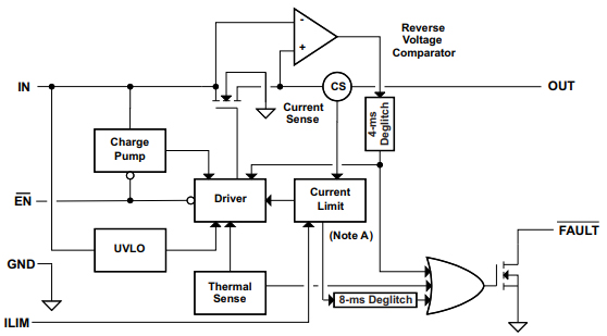
TPS2553DBVR Functional Block Diagram

The following figure is TPS2553DBVR Functional Block Diagram.

Functional Block Diagram

TPS2553DBVR Layout

Layout Guidelines

• The 100-nF bypass capacitor should be placed near the IN and  GND  pins, and the connections should be made with a low-inductance trace, according to TI.

• When substantial transient currents are predicted on the output, TI suggests using a high-value electrolytic capacitor and a 100-nF bypass capacitor on the output pin.

• To avoid parasitic effects on the current limit accuracy, the traces routing the RILIM resistor to the device must be as short as feasible.

• A wide and short copper trace must be used to link the PowerPAD to the PCB ground plane.

Layout

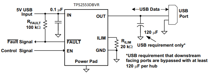
TPS2553DBVR Typical Application

The TPS2553DBVR Typical Application is shown as follows.

Typical Application


Depending on the external system conditions, some applications require varying current-limit thresholds. An implementation for an externally controlled, two-level current-limit circuit is shown in the diagram below. The total resistance from ILIM to GND determines the current-limit threshold. MOSFET Q1 is enabled or disabled by a logic-level input, and the current-limit threshold is changed by changing the total resistance from ILIM to GND. To expand the number of extra current-limit levels, more MOSFET and resistor combinations can be utilized in parallel with Q1/R2.

Two-Level Current-Limit Circuit

TPS2553DBVR Alternatives

Part Number Description Manufacturer
TPS2553DBVTPOWER CIRCUITS 0.075-1.7A adj. ILIMIT, 2.5-6.5V, 85mΩ USB power switch, active-high, reverse blocking 6-SOT-23 -40 to 125 Texas Instruments

TPS2553DBVR Applications

• USB Ports and Hubs

• Digital TVs

• Set-Top Boxes

• VOIP Phones

• Power Management


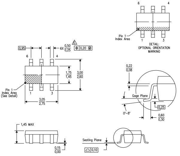
TPS2553DBVR Package

The following shows TPS2553DBVR Package.

Package

TPS2553DBVR Manufacturer

As a global semiconductor company operating in 35 countries, Texas Instruments (TI) is first and foremost a reflection of its people. From the TIer who unveiled the first working integrated circuit in 1958 to the more than 30,000 TIers around the world today who design, manufacture and sell analog and embedded processing chips, we are problem-solvers collaborating to change the world through technology.


Datasheet PDF

TPS2553DBVR Documents

Download datasheets and manufacturer documentation for TPS2553DBVR

Frequently Asked Questions

What is a current limited power switch?
When continuous heavy overloads and short-circuits increase the power dissipation in the switch, causing the junction temperature to rise, a thermal protection circuit shuts off the switch to prevent damage. This power-distribution switch is designed to set the current limit at 0.5 A typically.
How does current limiting work?
As the name suggests, the current limiting circuit limits the current from the regulated power supply to a maximum amount determined by the circuit, and in this way, severe damage to the circuits, both the power supply and the circuit being powered can be avoided.
How much continuous load current does the TPS2553DBVR power-distribution switch provide?
1.5 A.
What device provides a configurable current-limit threshold between 75 mA and 1.7 A?
External resistor.
What is the current-limit accuracy of the TPS2553DBVR power-distribution switch?
6%.
What is the purpose of the TPS2553DBVR power-distribution switch?
Reduce current surges.
What mode does the TPS2553DBVR device use to limit the output current to a safe level?
Constant-current mode.
What disables the power switch when the output voltage is driven higher than the input voltage?
An inbuilt reverse-voltage comparator.
What asserts low during overcurrent and reverse-voltage circumstances?
FAULT output.
FAQ
What is a current limited power switch?
When continuous heavy overloads and short-circuits increase the power dissipation in the switch, causing the junction temperature to rise, a thermal protection circuit shuts off the switch to prevent damage. This power-distribution switch is designed to set the current limit at 0.5 A typically.
How does current limiting work?
As the name suggests, the current limiting circuit limits the current from the regulated power supply to a maximum amount determined by the circuit, and in this way, severe damage to the circuits, both the power supply and the circuit being powered can be avoided.
How much continuous load current does the TPS2553DBVR power-distribution switch provide?
1.5 A.
What device provides a configurable current-limit threshold between 75 mA and 1.7 A?
External resistor.
What is the current-limit accuracy of the TPS2553DBVR power-distribution switch?
6%.
What is the purpose of the TPS2553DBVR power-distribution switch?
Reduce current surges.
What mode does the TPS2553DBVR device use to limit the output current to a safe level?
Constant-current mode.
What disables the power switch when the output voltage is driven higher than the input voltage?
An inbuilt reverse-voltage comparator.
What asserts low during overcurrent and reverse-voltage circumstances?
FAULT output.

TAGS

Share