ATTENTION: Due to increased demand and order volume, processing time may take an additional 1-3 business days.
HomeCommunitySubjectTPS27081ADDCR High-Side Load Switch: Diagram, Pinout, and Datasheet

TPS27081ADDCR High-Side Load Switch: Diagram, Pinout, and Datasheet

The TPS27081ADDCR is a load switch that can handle up to 8 volts and 3 amps. This article mainly introduces Diagram, Pinout, Datasheet and other detailed information about Texas Instruments TPS27081ADDCR.

600

Mar 14, 2022

Bernie Yale

Transistor as a switch - low side or high side


The TPS27081ADDCR is a load switch that can handle up to 8 volts and 3 amps. This article mainly introduces Diagram, Pinout, Datasheet and other detailed information about Texas Instruments TPS27081ADDCR.

TPS27081ADDCR

Inquiry
Min.: 1 Mult.: 1
Quantity Unit Price Ext. Price
1+ $8.6$8.6
10+ $6.13$61.3
25+ $5.52$138
100+ $4.847$484.7
250+ $4.526$1131.5
500+ $4.332$2166
1000+ $4.1769$4176.9
Looking for a better price? Want a lower wholesale price? Please send an RFQ, and we will respond immediately.
Quick Links

TPS27081ADDCR Description

The TPS27081ADDCR is a load switch that can handle up to 8 volts and 3 amps. The device uses an ultra-low resistance P-channel MOSFET to reduce voltage drop for low voltage and high current rails, lowering the dropout voltage via the device.

The device includes a customizable slew rate that aids in reducing or eliminating power supply droop caused by large inrush currents. The device exhibits very low leakage currents when it is turned off.

The TPS27081ADDCR combines a Power PFET and a Control NFET into a single small package, and has ESD protection on all pins, allowing for better ESD compatibility with other onboard components.

The TPS27081ADDCR level shifts ON/OFF  logic signals to VIN levels and supports CPU or MCU logic as low as 1-V to manage higher voltage power sources without the need for an external level-shifter.

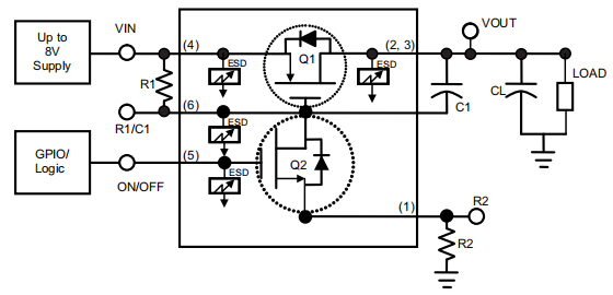
Using a quick ON/OFF  logic signal to switch a large value output capacitor CL may result in an excessive inrush current. Connect a resistor R2 and an external capacitor C1 as illustrated in the Simplified Schematic to manage the load inrush current. Refer to the Application and Implementation section to set the TPS27081ADDCR to obtain a specific slew rate.

In standby power switch applications, a single pullup resistor R1 is required. When inrush current regulation is not required, connect the R2 pin of the TPS27081ADDCR to system ground in such situations.

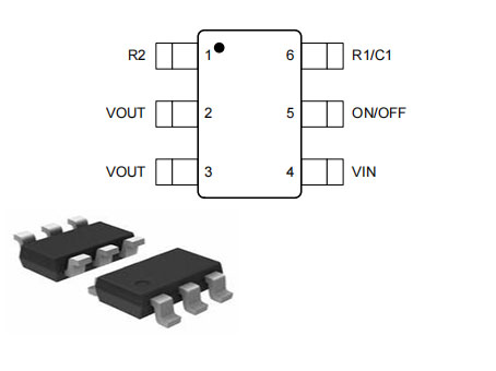
TPS27081ADDCR Pinout

The following shows TPS27081ADDCR Pinout.

Pinout


Pin Number Pin Name Description
5 ON/OFF Active high enable. When driven with a high-impedance driver, connect an external pull down resistor to GND
6 R1/C1 Gate terminal of power PFET (Q1)
1 R2 Source terminal of NMOS (Q2) . Connect to system GND directly or through a slew rate control resistor
4 VIN Source terminal of power PFET (Q1). Connect a pull-up resistor between the pins VIN/R1 and R1/C1
2,3 VOUT Drain terminal of power PFET (Q1). Connect a slew control capacitor between pins VOUT and R1/C1

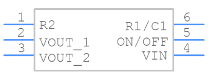
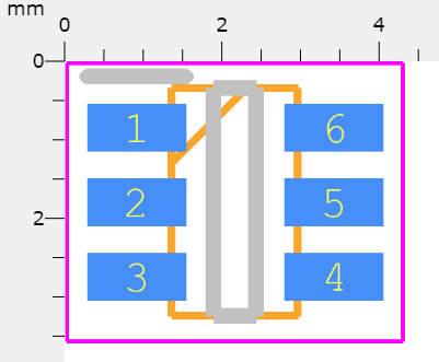
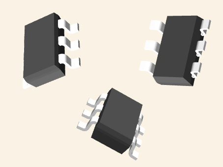
TPS27081ADDCR CAD Model

The followings are TPS27081ADDCR Symbol, Footprint and 3D Model.

Symbol

Footprint

3D Model

TPS27081ADDCR Features

• Low ON-Resistance, High-Current PFET

– RDS(on) = 32 mΩ at VGS = –4.5 V

– RDS(on) = 44 mΩ at VGS = –3 V

– RDS(on) = 82 mΩ at VGS = –1.8 V

– RDS(on) = 93 mΩ at VGS = –1.5 V

– RDS(on) = 155 mΩ at VGS = –1.2 V

• Adjustable Turnon and Turnoff Slew Rate Control Through External R1, R2, and C1

• Supports a Wide Range of 1.2-V to 8-V Supply Inputs

• Integrated  NMOS  for PFET Control

• NMOS ON/OFF Supports a Wide Range of 1-V to 8-V Control Logic Interface

• Full ESD Protection (All Pins)

– HBM 2 kV, CDM 500 V

• Ultra-Low Leakage Current in Standby (Typical 100 nA)

• Available in Tiny 6-Pin Package

– 2.9 mm × 2.8 mm × 0.75 mm SOT (DDC)

Specifications

TPS27081ADDCR Tech Specifications

Texas Instruments TPS27081ADDCR technical specifications, attributes, parameters and parts with similar specifications to Texas Instruments TPS27081ADDCR.

Product Attribute Attribute Value
Lifecycle StatusACTIVE (Last Updated: 5 days ago)
Factory Lead Time6 Weeks
MountSurface Mount
Mounting TypeSurface Mount
Package / CaseSOT-23-6 Thin, TSOT-23-6
Number of Pins6Pins
Weight36.003894mg
Operating Temperature-40°C~85°C TA
PackagingCut Tape (CT)
JESD-609 Codee3
Pbfree Codeyes
Part StatusActive
Moisture Sensitivity Level (MSL)1 (Unlimited)
Number of Terminations6Terminations
ECCN CodeEAR99
Resistance82mOhm
Terminal FinishMatte Tin (Sn)
Product Attribute Attribute Value
Max Power Dissipation1.19W
Terminal PositionDUAL
Terminal FormGULL WING
Peak Reflow Temperature (Cel)260
Number of Functions1Function
Supply Voltage5V
Terminal Pitch0.95mm
Base Part NumberTPS27081
Number of Outputs1Output
Max Output Current3A
Supply Voltage-Max (Vsup)8V
Supply Voltage-Min (Vsup)1V
InterfaceOn/Off
Output ConfigurationHigh Side
Power Dissipation1.19W
Output Current3A
Voltage - Supply (Vcc/Vdd)Not Required
Product Attribute Attribute Value
Switch TypeGeneral Purpose
Nominal Input Voltage8V
Ratio - Input:Output1:1
Voltage - Load1.2V~8V
Number of Drivers2Drivers
Rds On (Typ)32m Ω
Built-in ProtectionsTRANSIENT
FeaturesSlew Rate Controlled
Height1.1mm
Length2.9mm
Width1.6mm
Thickness870μm
REACH SVHCNo SVHC
Radiation HardeningNo
RoHS StatusROHS3 Compliant
Lead FreeLead Free
0 Products View Similar

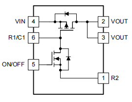
TPS27081ADDCR Functional Block Diagram

The following figure is TPS27081ADDCR Functional Block Diagram.

Functional Block Diagram

TPS27081ADDCR Simplified Schematic

The TPS27081ADDCR Simplified Schematic is shown as follows.

Simplified Schematic


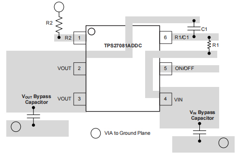
TPS27081ADDCR Layout

Use proper PCB layout techniques for the device's optimal operating performance, such as: 

•  VIN  and VOUT traces should be as short and wide as feasible to allow high current.

• Ceramic bypass capacitors with low ESR should be used to connect the VIN pin to ground. 1-F ceramic with X5R or X7R dielectric is a standard recommended bypass capacitance. This capacitor should be as close as feasible to the device pins.

• Ceramic bypass capacitors with low ESR should be used to connect the VOUT pin to ground. The suggested bypass capacitance is one-tenth of the VIN bypass capacitor with dielectric ratings of X5R or X7R.

This capacitor should be as close as feasible to the device pins.

Layout

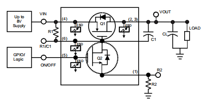
TPS27081ADDCR Typical Application

Standard Load Switching Application

The TPS27081ADDCR is a high-side load switch with a power PFET and a control NMOS integrated in a small package. Internal components of the device are rated for an 8-V supply and can handle up to 3 A of load current.

The device can be used for a wide range of purposes. The TPS27081ADDCR device is used to manage the load inrush current as shown in the diagram below.

Standard Application Diagram

TPS27081ADDCR Applications

• High-Side Load Switches

• Inrush Current Control

• Power Sequencing and Control

• Standby Power Isolation

• Portable Power Switches


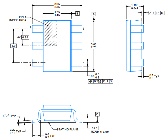
TPS27081ADDCR Package

The TPS27081ADDCR Package is shown as follows.

Package

TPS27081ADDCR Manufacturer

Texas Instruments Incorporated (TI) is an American technology corporation based in Dallas, Texas, that creates and manufactures semiconductors and integrated circuits for electronic designers and manufacturers around the world. Based on sales volume, it is one of the top ten semiconductor businesses in the world. Analog chips and embedded processors, which account for more than 80% of the company's revenue, are the company's main focus. TI also makes calculators, microcontrollers, and multi-core processors, as well as TI digital light processing technologies and education technology.


Datasheet PDF

TPS27081ADDCR Documents

Download datasheets and manufacturer documentation for TPS27081ADDCR

PCN Assembly/Origin
LBC7 Wafer Chg 15/Oct/2018

Frequently Asked Questions

What does a high side switch do?
High-side switches can safely drive high currents into complex (resistive, inductive, and capacitive) grounded loads in compliance with the harsh automotive environment. This requires both a robust, low on-resistance power switch and accurate analog circuitry for diagnostic, protection, and control functions.
What is the high and low side of a switch?
The low-side switch is switching ground while the high-side switch is connecting the voltage supply. Generally in a circuit, you want to keep the ground connected and switch the power.
What is load switching?
A load switch is simply a switch, mechanical or electronic, that connects or disconnects a load to the high side of a power source. A wall light switch is a load switch. Any off/on switch on an appliance or electronic product is a load switch. A relay can be a load switch.
How many volts does the TPS27081ADDCR handle?
8 volts and 3 amps.
What type of P-channel MOSFET does the TPS27081ADDCR use?
Ultra-low resistance.
What is the slew rate of the TPS27081ADDCR?
Reducing or eliminating power supply droop.
What does the TPS27081ADDCR exhibit when it is turned off?
Very low leakage currents.
What two components does the TPS27081ADDCR combine into a single small package?
Power PFET and a Control NFET.
What does the TPS27081ADDCR support as low as 1-V to manage higher voltage power sources without the need for an external level-shifter?
CPU or MCU logic.
What happens when using a quick ON/OFF logic signal to switch a large value output capacitor CL?
Using a quick ON/OFF logic signal to switch a large value output capacitor CL may result in an excessive inrush current.
In what document is the TPS27081ADDCR illustrated?
Simplified Schematic.
What section of the TPS27081ADDCR provides a specific slew rate?
Application and Implementation.
What is required in standby power switch applications?
A single pullup resistor R1.
What pin does the TPS27081ADDCR connect to when inrush current regulation is not required?
R2 pin.
FAQ
What does a high side switch do?
High-side switches can safely drive high currents into complex (resistive, inductive, and capacitive) grounded loads in compliance with the harsh automotive environment. This requires both a robust, low on-resistance power switch and accurate analog circuitry for diagnostic, protection, and control functions.
What is the high and low side of a switch?
The low-side switch is switching ground while the high-side switch is connecting the voltage supply. Generally in a circuit, you want to keep the ground connected and switch the power.
What is load switching?
A load switch is simply a switch, mechanical or electronic, that connects or disconnects a load to the high side of a power source. A wall light switch is a load switch. Any off/on switch on an appliance or electronic product is a load switch. A relay can be a load switch.
How many volts does the TPS27081ADDCR handle?
8 volts and 3 amps.
What type of P-channel MOSFET does the TPS27081ADDCR use?
Ultra-low resistance.
What is the slew rate of the TPS27081ADDCR?
Reducing or eliminating power supply droop.
What does the TPS27081ADDCR exhibit when it is turned off?
Very low leakage currents.
What two components does the TPS27081ADDCR combine into a single small package?
Power PFET and a Control NFET.
What does the TPS27081ADDCR support as low as 1-V to manage higher voltage power sources without the need for an external level-shifter?
CPU or MCU logic.
What happens when using a quick ON/OFF logic signal to switch a large value output capacitor CL?
Using a quick ON/OFF logic signal to switch a large value output capacitor CL may result in an excessive inrush current.
In what document is the TPS27081ADDCR illustrated?
Simplified Schematic.
What section of the TPS27081ADDCR provides a specific slew rate?
Application and Implementation.
What is required in standby power switch applications?
A single pullup resistor R1.
What pin does the TPS27081ADDCR connect to when inrush current regulation is not required?
R2 pin.

TAGS

Share