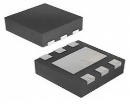
PMIC - LED Drivers 6-WDFN Exposed Pad -40°C~85°C TA Backlight 600kHz 3.6V TPS61161 IC LED DRVR RGLTR DIM 700MA 6SON
The TPS61161ADRVR is a boost converter that drives LEDs in series and has a 40-V rated integrated switch FET.

PMIC - LED Drivers 6-WDFN Exposed Pad -40°C~85°C TA Backlight 600kHz 3.6V TPS61161 IC LED DRVR RGLTR DIM 700MA 6SON The TPS61161ADRVR is a boost converter that drives LEDs in series and has a 40-V rated integrated switch FET.
316
Dec 3, 2021
Sara Sally
PMIC - LED Drivers 6-WDFN Exposed Pad -40°C~85°C TA Backlight 600kHz 3.6V TPS61161 IC LED DRVR RGLTR DIM 700MA 6SON
The TPS61161ADRVR is a boost converter that drives LEDs in series and has a 40-V rated integrated switch FET.
The TPS61161ADRVR is a boost converter that drives LEDs in series and has a 40-V rated integrated switch FET. To eliminate output ripple, enhance conversion efficiency, and allow for the use of small external components, the boost converter operates at a set switching frequency of 600kHz.
As demonstrated in the typical application, the default white LED current is set using the external sensor resistor Rset, and the feedback voltage is regulated to 200mV. During operation, a pulse width modulation (PWM) signal applied to the CTRL pin can regulate the LED current, with the duty cycle determining the feedback reference voltage. The TPS61161ADRVR does not burst the LED current in PWM dimming mode, hence there are no loud noises on the output capacitor. The device has an incorporated open LED protection function that disables the TPS61161ADRVR to prevent the output from exceeding the absolute maximum ratings under open LED conditions for maximum protection.
The TPS61161ADRVR is available in a space-saving, 2mm × 2mm QFN package with a thermal pad.
The Pinout of TPS61161ADRVR is shown as follows.
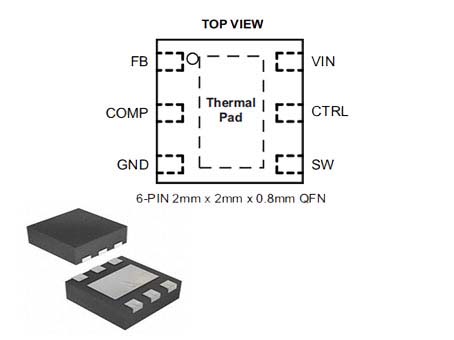
Pinout
| Pin Number | Pin Name | Description |
| 1 | FB | Feedback pin for current. Connect the sense resistor from FB to GND. |
| 2 | COMP | Output of the transconductance error amplifier. Connect an external capacitor to this pin to compensate the regulator. |
| 3 | GND | Ground |
| 4 | SW | This is the switching node of the IC. Connect the inductor between the VIN and SW pin. This pin is also used to sense the output voltage for open LED protection |
| 5 | CTRL | Control pin of the boost regulator. Enable and disable IC. PWM signal can be applied to the pin for LED brightness dimming as well. |
| 6 | VIN | The input supply pin for the IC. Connect VIN to a supply voltage between 2.7V and 18V. |
| Thermal Pad | The thermal pad should be soldered to the analog ground plane. If possible, use thermal via to connect to ground plane for ideal power dissipation. |
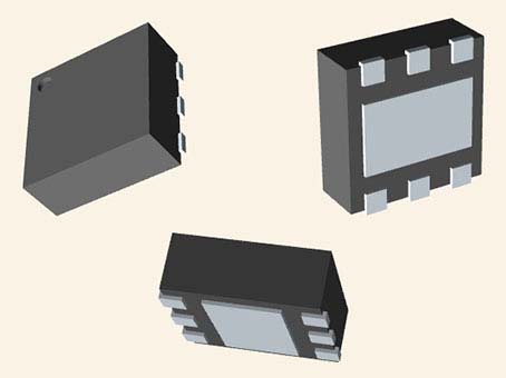
The following figures are TPS61161ADRVR Symbol, Footprint and 3D Model.
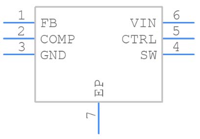
Symbol
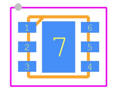
Footprint
3D Model
• 2.7V to 18V Input Voltage Range
• 38V Open LED Protection for TPS61161A
• 200mV Reference Voltage With ±2% Accuracy
• PWM Interface for Brightness Control
• Built-in Soft Start
• Up to 90% Efficiency
• 2mm × 2mm × 0.8mm 6-pin QFN Package With Thermal Pad
NA TPS61161ADRVR technical specifications, attributes, parameters and parts with similar specifications to NA TPS61161ADRVR.
undefined undefined technical specifications, attributes, parameters and parts with similar specifications to undefined undefined.
| Product Attribute | Attribute Value |
|---|
| Product Attribute | Attribute Value |
|---|
| Product Attribute | Attribute Value |
|---|
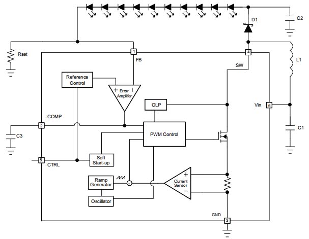
The following figure shows you the Block Diagram of TPS61161ADRVR.
Functional Block Diagram
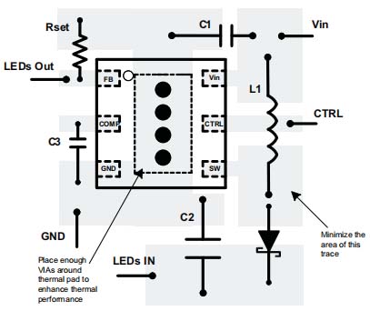
Layout is a key design phase for all switching power supplies, especially those with high frequency and high current. If the layout isn't done correctly, the regulator may have instability as well as noise issues.
The SW pin rise and fall timings are kept as short as feasible to prevent switching losses. The right layout of the high-frequency switching path is critical for preventing the radiation of high-frequency resonance problems.
To reduce inter-plane coupling, keep any traces linked to the SW pin as short and as little as possible. Always utilize a ground plane beneath the switching regulator. The PWM switch, Schottky diode, and output capacitor are all part of a loop that contains a lot of currents that rise and fall in nanoseconds and should be kept as brief as possible. In order to limit the IC supply ripple, the input capacitor must be close not only to the VIN pin but also to the GND pin. A sample arrangement is depicted in the accompanying figure.
Layout
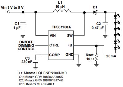
The following figures will show you TPS61161ADRVR Additional Typical Applications.
Li-Ion Driver for 6 White LEDs
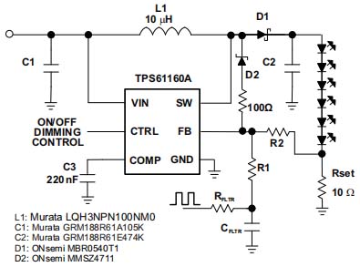
Li-Ion Driver for 6 White LEDs With External PWM Dimming Network
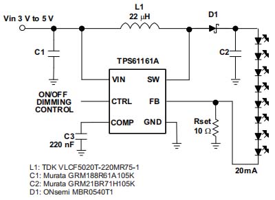
Li-Ion Driver for 8 White LEDs
• Cellular Phones
• Portable Media Players
• Ultra Mobile Devices
• GPS Receivers
• White LED Backlighting for Media Form Factor Display
The following figure is the Package of TPS61161ADRVR.
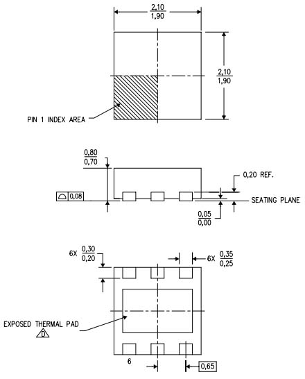
Package
Texas Instruments Incorporated (TI) is a Texas-based technology company that designs and manufactures semiconductors and integrated circuits for electronic designers and manufacturers all over the world. It is one of the top ten semiconductor companies in the world based on sales volume. The company's major focus is analog chips and embedded processors, which account for more than 80% of the company's sales. Calculators, microcontrollers, and multi-core processors, as well as TI digital light processing technologies and education technology, are all manufactured by TI. The company had 45,000 patents worldwide as of 2016.
Download datasheets and manufacturer documentation for
TAGS
Comments