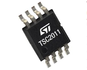
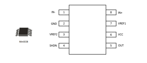
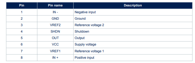
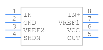
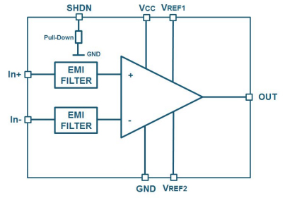
The TSC2011 is a fixed gain current sensing amplifier of 60 V/V. Thanks to a thin film resistor, the TSC2011 offers an extremely precise gain and a very high CMRR performance even in a high frequency range. Moreover, by fixing the output common mode voltage, the TSC2011 can be either used as unidirectional or bidirectional current sensing amplifier. The TSC2011 provides an extended input common range from -20 V below the negative supply voltage, and up to 70 V allowing either low-side or high-side current sensing, while the TSC2011 device can operate from 2.7 to 5.5 V. The parameters are very stable in the full Vcc range and characterization curves show the TSC2011 characteristics at 2.7 V and 5.0 V. Moreover, the main specifications are guaranteed in an extended temperature range from -40 to 125 ℃.
The main feature of the TSC2011 is the ability to work with an input common mode voltage largely beyond the power supply Vcc range (2.7 V to 5.5 V). It is ideal, for example for automotive applications where a reverse battery can be supported by the TSC2011 without any damage. It also works with 48 V battery applications as the TSC2011 can support and measure the current on line at voltage up to 70 V. No additional protective components are needed in that range.
Some ADCs get their signal thanks to a sample and hold capacitor. If before a sampling this capacitance is fully discharged, a fast current load can appear on the output of the TSC2011 during the sampling phase. The scope probe in the figure below shows the output voltage of the TSC2011 excited by a 40 pF capacitor with a 3.3 Vpp signal at 50 kHz to simulate the sample and hold circuit of the ADC120. The ADC120 has a conversion rate of 50 ksps, which is perfect to sample and hold the output of the TSC2011 without any error.
The graph shows the behavior of the output of the TSC2011 under the worst case condition, as for example, when there is an ADC120 channel change between two measurements. If a single channel is used, for sure the change on the sample and hold capacitance are very small, and so the recovery time is extremely low as described by the figure below. The effect of the ADC sampling and hold can be easily smoothed thanks to an RC filter. As suggested on the schematic below. The capacitor of the external filter must be chosen much higher than the internal ADC capacitor, in order to easily absorb the sudden voltage variation on the output due to the sampling and hold of the ADC. The resistance must be chosen accordingly to the application speed of the system in order not to impact the whole application. The main advantage of using an RC filter is to have an antialiasing system. For sure the used ADC must have sample and hold conversion in accordance with the RC filter value, in order to let the output recover before sampling.