
Introduction
An analog-to-digital converter, or A/D converter, or ADC for short, usually refers to an electronic device that converts an analog signal into a digital signal. Except for the most specialized analog-to-digital converters, all ADCs are implemented as integrated circuits (ICs). These are usually mixed-signal integrated circuit chips based on metal oxide semiconductor (MOS) that integrate analog and digital circuits.
As we all know, ADC is mainly used to the digital acquisition of analog signals for for data processing purposes. The signals around us are generally continuously changing analog quantities, such as light, temperature, speed, pressure, sound, etc. However, most of us use digital equipment. If we want to use and process information easily, it is necessary to convert the analog quantity into a digital quantity and transmit it to the microcontroller or microprocessor. So how is ADC conversion realized? What kind of process is it? Reading the following note, you will definitely have a more comprehensive and systematic understanding of the analog-to-digital converter.
What is ADC (Analog to Digital Converter)?
Ⅰ A/D Converter Basic
1.1 Analog-to-Digital Converter Definition
The ADC converter is a system that converts analog signals into digital signals. It is a process of filtering, sample-and-hold, quantization and encoding. The analog signal passes band-limited filtering, sample-and-hold circuit, and becomes a ladder-shaped signal, and then passes through the encoder to make each level in the ladder-shaped signal become a binary code. Finally, the analog quantity is converted into a digital quantity and then transmitted to the CPU. That is to say, almost all energized data need ADC conversion. For example, electric energy metering of electric energy meters, weight measurement of electronic scales, temperature measurement of electronic thermometers, and communication fields.
1.2 Analog to Digital Conversion Steps
The process of converting analog quantities into digital quantities is called analog-to-digital conversion, abbreviated as A/D, and the circuit that completes this function is called analog-to-digital converter, or ADC for short.
Analog-to-Digital Conversion Steps Animation
1) Sampling refers to replacing the original continuous signal in time with a sequence of signal samples at regular intervals, that is, discretizing the analog signal in time.
2) Quantization uses a limited number of amplitude values to approximate the original continuously changing amplitude value, that is, changing the continuous amplitude of the analog signal into a limited number of discrete values with a certain interval.
3) Encoding is based on a certain rule, the quantized value is represented by binary numbers, and then converted into a binary or multi-value digital signal stream. The digital signal obtained in this way can be transmitted through digital lines such as cables, microwave trunk lines, and satellite channels.
The higher the signal frequency, the higher the operating frequency of the A/D circuit. The more digits, the more accurate the restoration accuracy of the signal. The I/O port of the MCU needs program cooperation to complete the A/D conversion. What’s more, the A/D chip can also be used alone to complete the analog-to-digital conversion.
1.3 Why do We Need Analog-to-Digital Converter?
Computer software, radio, and digital image acquisition all need the assistance of ADC converters, that is, the wave of human digitization has promoted the invention, development and continuous change of ADC converters. In short, the ADC converter plays an important role in human digitization.
1) Many recording studios use 24-bit/96 kHz (or higher) pulse code modulation (PCM) or direct stream digital (DSD) recording formats, and then use ADC samples or decimates the signal for digital audio production on discs.
2) Use ADC to store or transmit almost any analog signal in digital form. For example, TV tuner cards use fast video analog-to-digital converters. Digital storage oscilloscopes require very fast analog-to-digital converters, and ADCs are also crucial for software-defined radio and its new applications.
3) Digital imaging systems usually use analog-to-digital converters to digitize pixels. Some radar systems usually use ADCs to convert signal strength into digital values for subsequent signal processing.
4) Certain non-electronic or only partially electronic devices (such as rotary encoders) can also be regarded as analog-to-digital converters.

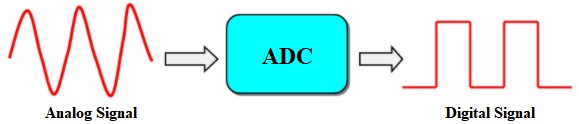
Figure 1. Analog to Digital Conversion Example(Light Signal to Digital Signal)
Ⅱ Which A/D Converter is Better?
After years of development and continuous technological innovation, ADC converters have developed from Flash ADCs, Successive-Approximation ADCs, Counting/Slope Integration ADCs to sigma-delta (Σ-Δ) ADCs and Pipelined ADCs. They have their own advantages and disadvantages, and they can also meet different requirements.
Successive-Approximation ADCs, Counting/Slope Integration ADCs and compression ADCs, etc. are mainly used in low-speed or medium-speed, medium-precision data acquisition and intelligent instruments. Hierarchical and pipelined ADCs are mainly used in high- speed signal processing, fast waveform storage and data recording, etc., such as video signal quantization and high-speed digital communication technology. ∑-△ ADC is mainly used in high-precision data acquisition, especially in electronic measurement fields such as digital sound systems, multimedia, seismic exploration instruments, sonar and so on. Here a brief description of the main ADC types is given below.
- Successive-Approximation ADC
The successive-approximation ADC is widely used. It includes a comparator, a digital-to-analog converter, a successive-approximation register (SAR) and a control logic unit. It is to continuously compare the sampling input signal with the known voltage. One clock cycle completes the 1-bit conversion, and the N-bit conversion requires N clock cycles. The conversion is completed and the output binary number is output. The resolution and sampling rate of this type ADC are contradictory: when the ADC resolution is low, the sampling rate is high, and if the resolution is to be improved, the sampling rate will be limited.
Advantages: when the resolution is lower than 12 bits, the price is cheap, and the sampling rate can reach 1MSPS. Compared with other types, the power consumption is quite low.
Disadvantages: In the case of higher than 14-bit resolution, the price is higher. The signal generated by the sensor needs to be conditioned before analog-to-digital conversion, including gain stage and filtering, so that the cost will increase significantly.
- Counting/Slope Integration ADCs
Counting/Slope Integration ADC is also called dual-slope or multi-slope ADC, and its applications are also very wide. It is composed of an analog integrator with an input switch, a comparator and a counting unit. The input analog voltage is converted into a time interval proportional to its average value through two integrations. At the same time, a counter is used to count the clock pulses in this time interval, so as to realize the analog-to-digital conversion. Because the input end applies the integrator, it has a strong ability to suppress the interference of AC noise. For example, for high-frequency noise and fixed low-frequency (50Hz or 60Hz) interference suppression, it is suitable for use in noisy industrial environments. This type ADC is mainly used in low-speed, precision measurement and other fields, such as digital voltmeters.
Advantages: High resolution, up to 22 bits; low power consumption and low cost.
Disadvantages: The conversion rate is low, 100~300SPS at 12 bits.
- Parallel ADCs
The main feature of inter ADC is fast speed, which is the fastest of all types. The sampling rate can reach above 1GSPS. However, due to the limitations of power and volume, it is difficult to improve the resolution. The conversion of all bits of the ADC with this structure is completed at the same time, and the conversion time mainly depends on the switching speed of the comparator and the transmission time delay of the encoder. In addition, increasing the output code has little effect on the conversion time, but as the resolution increases, a high-density analog design requires large number of precision divider resistors and comparator circuits for the conversion. That is to say, the output number is increased by one bit and the number of precision resistors is increased. It is about to double, and the comparator is also approximately doubled.
The resolution of the parallel comparison ADC is limited by die size, input capacitance, power, etc. If the accuracy of the parallel comparators does not match, it will also cause static errors and increase the input offset voltage.
- Sigma-delta (Σ-Δ) ADCs
The Sigma-delta (Σ-Δ) ADC is composed of an integrator, a comparator, a 1-bit DA converter, and a digital filter. In principle, it is similar to the integral type. The input voltage is converted into a time (pulse width) signal and processed by a digital filter to obtain a digital value.
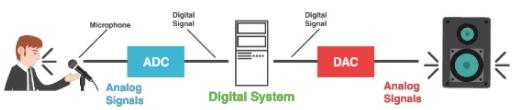
Figure 2. Analog to Digital Converter Application Example
Ⅲ What A/D Converter Includes?
1) Sampling Rate
The sampling rate indicates the rate at which the analog signal is converted into a digital signal, which is related to the manufacturing technology of the ADC device and depends on the judgment ability provided by the comparator in the ADC.
Generally speaking, the sampling rate and resolution are mutually restrictive. Each time the sampling rate is doubled, the resolution losses 1bit. This is mainly due to the jitter during sampling, that is, aperture jitter or aperture uncertainty.
2) ADC Resolution
The resolution indicates the number of bits after the analog signal is converted into a digital signal. It directly determines the quantization level of the ADC, that is, the minimum analog signal level value that the ADC can distinguish. Assuming that the ADC's input voltage range is (−V, V) and the resolution is N (bit), then the ADC has a 2N quantization level, so that the quantization level is: ΔV=2V/2N, where ΔV is the conversion accuracy. It can be seen from the above formula that the higher the resolution of the ADC and the smaller the voltage input range, the higher its conversion accuracy.
3) Signal-to-Noise Ratio (SNR)
The signal-to-noise ratio (SNR) of the ADC reflects the ratio of the root mean square value of the noise-free signal part generated during the quantization process to the root mean square value of the quantization noise. If the input signal is a normalized sine wave 1/2sin(ωt ψ), the SNR can be determined by the following formula: 
Among them, N is the resolution of ADC. It can be seen that the signal-to-noise ratio of the ADC mainly depends on the resolution. Every time the resolution increases by one bit, the SNR will increase by 6dB. However, as the resolution increases, the quantization level of the ADC becomes smaller, and the sampling process is more likely to be disturbed.
4) Effective Number of Bits (ENOB)
ENOB is a measure of the dynamic range of an ADC converter. For the actual A/D conversion system, due to the influence of factors such as electrical noise, external interference, and non-linear distortion of analog circuits, it is not enough to measure system performance with ideal resolution. In order to better reflect the system performance, on the basis of the measured SNR, the above factors can be converted into quantization noise to get the ENOB. The calculation formula is as follows: 
ENOB is based on the equation for an ideal ADC's SNR: SNR = 6.02 × N 1.76 dB, where N is the ADC's resolution.The difference between ENOB and ADC resolution reflects the degree of decrease in sampling accuracy caused by the decrease in SNR(here SNR caused by the error source).
5) Non-Linearity Error
Non-linear error is an important accuracy index of the converter, which represents the difference between the actual conversion value of the ADC and the theoretical conversion value. Non-linear errors mainly include two types: Differential Non-Linearity (DNL) errors and Integral Non-Linearity (INL) errors.
6) Inter Modulation Distortion (IMD)
When two sinusoidal signals are input to the ADC at the same time, due to the nonlinearity of the device, except the components of these two frequencies, the output spectrum will also produce many distortion products. The resulting distortion is called inter modulation distortion ( IMD, Inter Modulation Distortion), where the value of m n represents the order of distortion. Among all inter-modulation distortions, the second-order and third-order inter-modulation products are the most important. The former is easily filtered out by a digital filter, while the latter is difficult to filter out.
7) Total Harmonic Distortion (THD)
Due to the nonlinearity of the ADC, many high-order harmonics of the input signal appear in the output spectrum. These high-order harmonic components are called harmonic distortion components, and the resulting distortion is called Total Harmonic Distortion. Harmonic distortion and modulation distortion are two different concepts. The former is a distortion of the original signal waveform, even if a single frequency signal passes through the ADC, this phenomenon will occur, while the latter is mutual interference and influence between different frequencies.
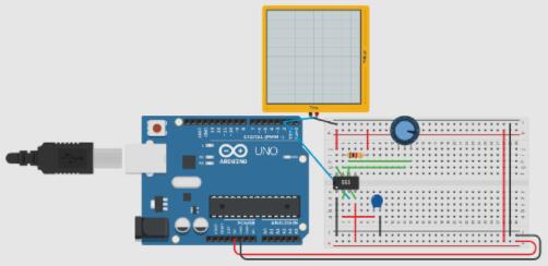
Figure 3. ADC on the Arduino
Ⅳ A/D Converter Applications and ICs
4.1 Analog-to-Digital Converter Applications
Most ADC applications today belong to Four Segments:
(a) Data acquisition
(b) Precision industrial measurement
(c) Voiceband and audio
(d) High speed (sampling rates greater than about 5 MSPS)
4.2 Analog-to-Digital Converter IC Modes Explained
There are many ADC ICs available in the market which can be used along to do conversion. Here lists several ADC ICs and their features and specifications as ADC selection references.
|
16-Bit, 2 LSB INL, 3 MSPS PulSAR® ADC, High sampling rate, Available in a 48-lead LQFP or a 48-lead LFCSP |
⭕AD7641 18-Bit, 2 MSPS, Charge Redistribution SAR ADC
|
3 MSPS (Wideband Warp and Warp Mode) 2 MSPS (Normal Mode) 1.25 MSPS (Impulse Mode)
|
2 MSPS (Warp mode) 1.5 MSPS (Normal mode)
|
|
⭕AD7908 8-Channel, 1 MSPS, 8-Bit ADC with Sequencer in 20-Lead TSSOP |
⭕AD7918 8-Channel, 1 MSPS, 10-Bit ADC with Sequencer in 20-Lead TSSOP |
6.0 mW max at 1 MSPS with 3 V supply 13.5 mW max at 1 MSPS with 5 V supply
|
6.0 mW max at 1 MSPS with 3 V supply 13.5 mW max at 1 MSPS with 5 V supply
|
|
⭕AD7928 8-Channel, 1 MSPS, 12-Bit ADC with Sequencer in 20-Lead TSSOP |
⭕AD5555 Precision DUAL 16-Bit 14-Bit-DACs in Compact TSSOP Packages |
6.0 mW max at 1 MSPS with 3 V supply 13.5 mW max at 1 MSPS with 5 V supply
|
|
|
⭕AD8230 16 V Rail-to-Rail, Zero-Drift, Precision Instrumentation Amplifier |
⭕AD7799 3-Channel, Low Noise, Low Power, 24-Bit, Sigma Delta ADC with On-Chip In-Amp |
110 dB minimum CMR @ 60 Hz, G = 10 to 1000 10 μV maximum offset voltage (RTI, ±5 V operation) 50 nV/°C maximum offset drift 20 ppm maximum gain nonlinearity |
27 nV at 4.17 Hz (AD7799) 65 nV at 16.7 Hz (AD7799) 40 nV at 4.17 Hz (AD7798) 85 nV at 16.7 Hz (AD7798)
|
|
⭕AD9444 14-Bit, 80 MSPS A/D Converter |
14-Bit, 105 MSPS / 125 MSPS A/D Converter |
DNL = ±0.4 LSB typical INL = ±0.6 LSB typical
|
DNL = ±0.25 LSB typical INL = ±0.8 LSB typical
|
|
⭕AD9446 16-Bit, 80 MSPS / 100 MSPS A/D Converter |
12-Bit, 20/40/65 MSPS, 3 V Analog-to-Digital Converter |
(3.8 V p-p input, 80 MSPS)
(3.2 V p-p input, 80 MSPS)
(3.2 V p-p input, 80 MSPS)
10.8 MHz (100 MSPS) l 60 fsec rms jitter
DNL = DNL = ±0.4 LSB typical INL = ±3.0 LSB typical
|
|