
Although silicon has long been the main semiconductor used in these applications, medium-voltage silicon carbide MOSFET power modules are becoming the best solution to replace current Si IGBT modules thanks to the superior static and dynamic performance offered by SiC.
High energy efficiency is crucial for several high-current power applications, including industry motor drives, renewable energy systems, and solid-state transformers. Although silicon has long been the main semiconductor used in these applications, medium-voltage silicon carbide MOSFET power modules are becoming the best solution to replace current Si IGBT modules thanks to the superior static and dynamic performance offered by SiC.
Medium-voltage SiC MOSFET and JFET devices have been developed by several vendors, with voltages ranging from 3.3 kV to 15 kV, as well as 3.3-kV SiC MOSFETs based on single-chip technology.2 This article will focus on a 7.2-kV/60-A SiC Austin SuperMOS switch, based on the series connection of 1.2-kV SiC MOSFETs. A novel 3.6-kV/400-A half-bridge intelligent power module (IPM) will be introduced to demonstrate the scalability of the SuperMOS concept. (The original article can be found here.1)
The circuit
The half-bridge upper and lower gate drivers are powered by a high-voltage isolated power supply (shown in Figure 1), based on a matrix transformer LLC converter with 10-kV isolation.3
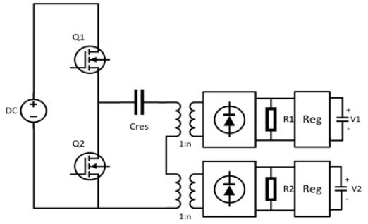
The half-bridge IPM comprises an LLC resonant converter and two rectifier units (upper and lower side), which are supplied via two high-frequency transformers, each of which consists of a toroid core enclosed in a custom 3D-printed bobbin with the secondary winding wound on the core. The high-voltage primary winding achieves a rated isolation voltage of 30 kV using silicone rubber as insulation material. The intelligent gate driver is optically triggered and features intelligent undervoltage lockout and overcurrent and overtemperature protection.
The module
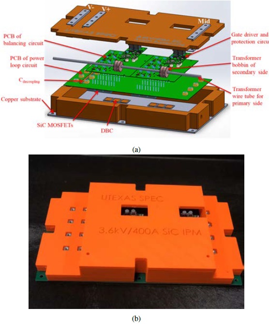
The proposed 3.6-kV/400-A half-bridge power module is shown in Figure 2a (exploded view) and Figure 2b (prototype). It has three high-power connections (VDC , VDC–, and SW node) and four optical fiber connections for two PWM inputs and two fault outputs. Integrating 12 1,200-V SiC MOSFETs based on the Austin SuperMOS configuration,4 the module uses a dedicated PCB to create a low-inductance power loop and has internal decoupling capacitors and a SuperMOS voltage-balancing circuit. The power-loop structure is designed with a magnetic flux cancellation effect to achieve low parasitic inductance. The discrete SiC MOSFET substrate was realized with a 1-mm–thickness aluminum nitride (AIN) direct-bonded copper, thus increasing both heat dissipation and insulation voltage.
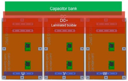
With the addition of some external DC capacitors, the IPM can be easily interfaced with a digital controller to form a three-phase system, as shown in Figure 3.
The IPM internal layout is shown in Figure 4. Both upper and lower devices comprise four branches of SuperMOS, each of which includes three 1.2-kV SiC MOSFETs.
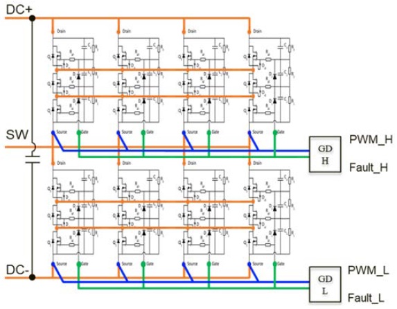
A detailed view of a single branch is shown in Figure 5. R1–R3 are 1-MΩ resistors required to achieve the static voltage balance, while C1–C3 are used for both dynamic voltage balancing and as part of the turn-on gate circuits for upper switches Q2–Q3. Rg2–Rg3 resistors are used to limit the charging and discharging currents in the gate branch during switching, while Dz2–Dz3 are Zener diodes for clamping the gate voltages of Q2–Q3. Finally, D1–D2 are 1-kV avalanche diodes for voltage clamping and to enhance the gate driver performance during turn-on.
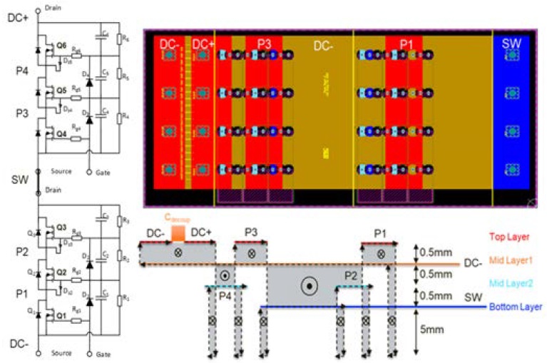
When a positive gate signal is applied to its gate, Q1 turns on. Its drain-to-source voltage (VDS) tends to fall, decreasing the potential of Q2’s source, as the gate-to-source voltage (VGS) of Q2 becomes positive. Upon reaching the threshold voltage (VTH), Q2 starts to turn on and its VDS starts to fall subsequently, turning on Q3. To switch off the module, a negative gate driver signal shall be applied to Q1’s gate, turning it off. Its VDS starts to increase, leading to a negative VGS being applied to Q2. When Q2’s VGS reaches its threshold voltage, it switches off, and its VDS starts to increase, leading to the turn-off of Q3.
To reduce the internal voltage overshoot, a power loop with an extremely low stray inductance is required. To achieve an ultra-low stray inductance, a magnetic cancellation effect of the current is applied. Q3D simulation has shown that the loop inductance is equal to 35 nH, including PCB and inductance from the discrete SiC MOSFETs. Inductance could be further reduced by replacing the discrete MOSFETs with bare die chips.
Performance measurement
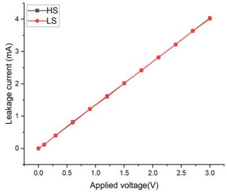
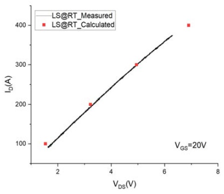
All performance measurements were performed at room temperature. Figure 6 shows the leakage current as a function of the applied voltage. At 3 kV, its value is 4 mA for both the lower (low-side) and upper (high-side) switches, mainly due to the static balancing resistors. However, its value can be reduced by using larger resistors. Figure 7 shows instead the measured and calculated forward-conduction characteristics at VGS = 20 V. At room temperature, the IPM calculated on-resistance is 16.75 mΩ.
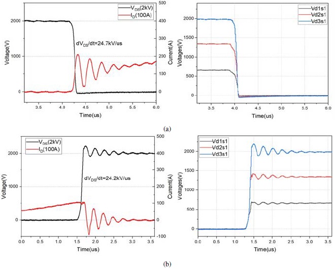
Regarding the dynamic performance, it has been characterized at room temperature using a double-pulse tester. Turn-on and turn-off waveforms, as well as the dynamic performance during 2-kV/100-A switching, are shown in Figure 8.
The turn-off waveforms at 2 kV/200 A and 2 kV/380 A, respectively, are shown in Figure 9. The SiC MOSFET changing rate of the drain-to-source voltage during the switching transient (dV/dt) was 30.7 kV/s and 38.9 kV/s, respectively.
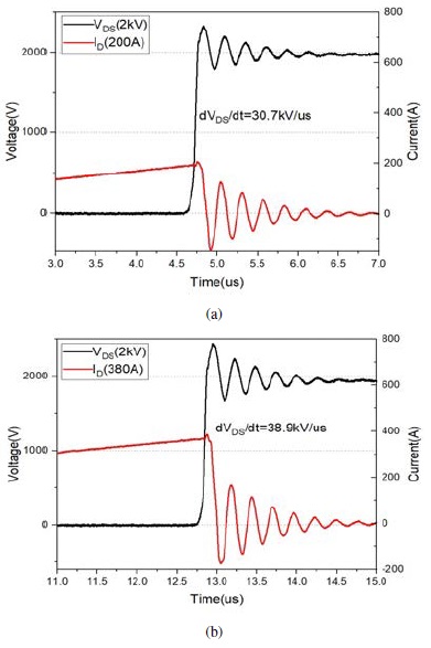
Experimental results confirm the excellent static and dynamic performances obtained by the IPM. As shown in Figures 8 and 9, experimental results confirm that the module achieves a reduced voltage overshooting, also confirming that the dynamic voltage balancing is well-achieved in the IPM at turn-on and turn-off transients.