
In recent years, the LiDAR technology has become the focus of attention, especially due to a high involvement of the automotive industry. Basically, a LiDAR system consists of a light emitter and a photo sensor. The distance to an obstacle is determined by measuring the time of flight from the emission of the light pulse to the detection of its reflection. Silicon Photomultipliers (SiPMs) are anticipated as LiDAR photo sensors capable of providing reliable and cost-effective long-distance ranging with low laser power due to a number of benefits.
These benefits include:
- A high photon detection efficiency at low thresholds for long range measurements,
- A high dynamic range to detect objects with highly different reflectivity and for the operation under strong ambient light,
- An excellent timing resolution for high precision measurements.
In this article, we present Ketek’s SiPM based on a 3D technology with an increased sensitivity in the visible to near-infrared wavelength range. The first prototypes show a superior photon detection efficiency (PDE) of 22% at the automotive LiDAR-typical wavelength of 905 nm, a single photon time resolution (SPTR) of about 0.5 ns, a high dynamic range and a fast recovery time.
The combination of these parameters makes our 3D-SiPM concept a suitable candidate for the detection of red and near-infrared wavelengths, especially in long range automotive LiDAR-systems. Also, application fields like robotics or consumer electronics may benefit from the improved detection capabilities.
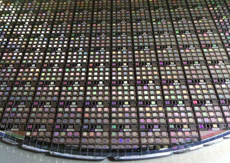
Advantages of silicon photomultipliers in LiDAR systems
One of the main quality factors of modern LiDAR systems in the automotive industry is the distance at which objects with a low reflectivity can be detected. Currently, the goal is to detect an object with 10% reflectivity in a distance of 300 m. To achieve this goal, the silicon photomultiplier (SiPM) is a detector of choice.
The SiPM is a semiconductor device which consists of an array of avalanche photodiodes (APD) connected in parallel and operated above their breakdown voltage, in Geiger-Mode (GM-APD). In this mode, the electric field exceeds a certain threshold and charge carriers, which are generated in the active area and can initiate a self-sustaining avalanche breakdown by the mechanisms of impact ionization. As a consequence, a breakdown current is flowing, which is large enough to be detected. In the following, the individual GM-APDs are referred to as micro-cells of the SiPM. Compared with commonly used APDs, the SiPM provides multiple advantages. The most prominent one is the ability to detect light intensities down to a level of one single photon with the use of simple front-end electronics. This ability is due to the high intrinsic gain in Geiger-Mode of the order of 104 to 107.
In contrast, typical APDs are designed to be operated in the so-called linear mode, where the intrinsic gain is of the order of 102 and the single photon detection capabilities are lost. A lower threshold for light detection directly translates into the range of the LiDAR-system, since the intensity of the emitted and reflected light signal is inversely proportional to the square of the distance. The typical operation voltages of a SiPM are in the range of 25 V to 50 V, which are significantly lower with respect to hundreds of volts that are required to operate an APD. This allows for much simpler biasing circuits.
Due to the intrinsic single photon time resolution of tens of picoseconds, the SiPM provides superior timing properties with respect to APDs. Additionally, the SiPM shows a much smaller temperature coefficient. Especially in automotive applications, the systems must operate in a wide temperature range. Independent of whether the photo sensor has a temperature stabilization/compensation or not, a low temperature coefficient of the breakdown voltage is beneficial.
For several years, Ketek has been providing state-of-the-art SiPMs based on planar pn-junctions. The sensors are optimized to have a detection peak in the blue range of the visible light spectrum, which is commonly used in medical applications. In automotive LiDAR- systems, near-infrared light, typically 905 nm is used for the excitation signal. To achieve high detection efficiencies for the red and near-infrared part of the light spectrum, a large detection volume is required due to the low absorption coefficient of silicon in this wavelength regime. Here, the planar technology inherits significant limitations. In the planar technology, the breakdown voltage increases proportionally to the depletion depth, leading to high operation voltages to reach the Geiger-Mode and to high temperature coefficients. Simultaneously, the lateral distance of the active volume to the micro-cell edge has to be increased in order to prevent edge breakdowns at high operation voltages. This significantly limits the geometric efficiency of the sensors and hence its light detection capabilities.
Next generation silicon photomultiplier concept
In order to overcome the limitations of the planar technology, Ketek developed a new 3D concept which utilizes a spherical depletion. As a consequence of the chosen geometry, the breakdown voltage is mainly determined by the radius of the spherical electrode and is nearly decoupled from the depth of the depletion region. In this way, it is possible to significantly increase the active volume in vertical direction and remain at sufficiently low breakdown voltages of about 50V. The focusing shape of the electric field and the lack of typical micro-cell edges allow to reduce inactive regions in lateral directions to a minimum. Since the design is not restricted by edge effects, a high-density micro-cell layout with a high geometric efficiency is accessible (see figure 2).
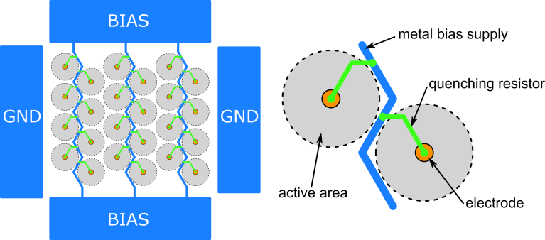
The current prototypes show a geometric efficiency above 80% for micro-cell pitches of 15 µm. This directly translates into an increased photon detection efficiency (PDE). The PDE describes the capability of the sensor to detect light as the ratio of the average number of incident and the average number of detected photons.
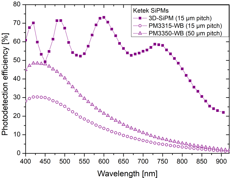
In figure 3, the PDE of Ketek’s 3D-SiPM and Ketek’s state-of-the-art planar SiPMs are compared at different wavelengths. The significantly higher PDE of the new prototypes in a wide spectral range can easily be observed. Ketek’s 3D-SiPM demonstrates the record peak PDE value of 73% at 600 nm with respect to state-of-the-art devices with a 15 µm pitch size. Additionally, the PDE curve does not show the typical fast decrease with increasing wavelengths and remains above a value of 45% up to a wavelength of 800 nm. At the LiDAR-wavelength of 905 nm, the PDE has a value of 22%, which is also the highest value reported so far. The oscillations in the PDE curve of the 3D-SiPM are caused by destructive interference due to the protective Si/SiO2 stack on top of the entrance window of the prototype devices.
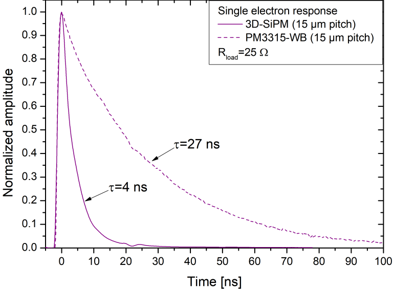
To achieve a sufficient ambient light immunity and a high photon count rate, a fast recovery of the micro-cells is required. The recovery time defines the time period in which a micro-cell is inactive after detecting a photon. In figure 4(a), the single photoelectron response of Ketek’s 3D-SiPM is shown. It was measured as the voltage drop across a 25 Ω load resistor. The shape of the single photoelectron response reflects the recovery process of the micro-cell. With the new concept, Ketek decreased the recovery time of each individual micro-cell down to 4 ns by a strongly reduced micro-cell capacity. As a consequence, the internal gain of the 3D-SiPM was reduced to the order of 5×10⁴. Compared to state of the art planar SiPMs, this is about a factor of 20 lower.
A further advantage of the low internal gain is that the readout electronics will saturate at higher photon numbers. This may provide additional linearity of the system.
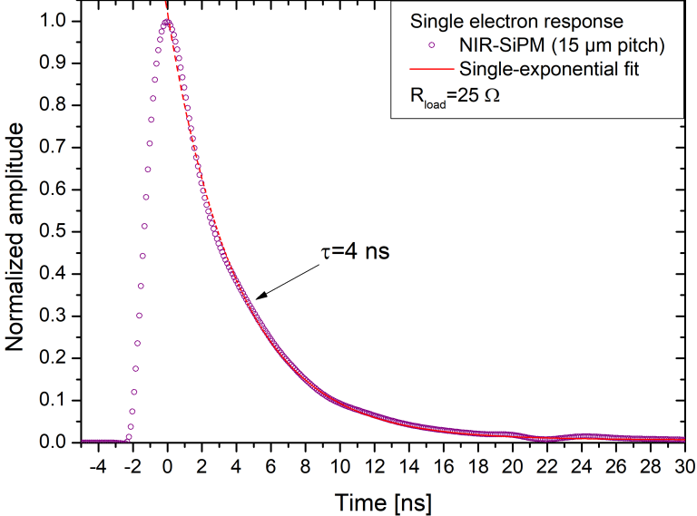
(a) SER of 3D-SiPM
(b) SER comparison
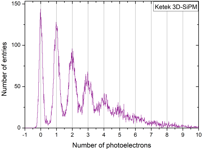
Figure 5 provides an example of a single photoelectron spectrum. The peaks up to 4 photoelectrons are well separated, making precise single photon counting possible.
Conclusion
With our new technology, Ketek has achieved a record photon detection efficiency over a wide spectral range from 400 nm to the LiDAR-typical 905 nm with a small micro-cell pitch of 15 µm. In combination with a high dynamic range, a fast recovery time (4 ns), and a low temperature coefficient of the breakdown voltage (26mV/K), this SiPM is a suitable detector for a large variety of applications. In the high-volume market, this sensor is suitable for automotive LiDAR applications.
Prototypes have already been tested in an existing modern LiDAR system under realistic environmental conditions. The preliminary results show that our 3D technology outperforms the state of the art SiPMs currently available on the market.