Power management ICs (PMICs) offer complete power management within a single chip. PMICs are often used to power small battery-powered devices, for which the integration of multiple functions increases efficiency in terms of space and power. Functions commonly integrated into a PMIC include voltage converters and regulators, battery chargers, battery fuel indicators, and LED drivers.
Low-power PMICs must offer compact form factors and high efficiency to provide long battery life in wearable devices. In computationally intensive systems such as systems-on-chip, FPGAs, and microcontrollers, the goal is to maximize performance per watt, again with an eye on optimizing system efficiency.
DC power management in electrically critical vehicle environments is not an issue that advanced driver assistance system (ADAS) designers can afford to ignore. PMIC solutions offer DC power protection, low quiescent current, and EMI reduction, providing a comforting environment for energy management in a vehicle.
The adoption of PMIC solutions in various devices has helped those platforms to use power efficiently and thus has extended their operating life. PMIC demand is expected to increase in the near future as designers look to bring advanced technology and features to products.
Challenges
As microelectronics shrink and power consumption requirements rise, power management is rising in complexity as well as importance. Wearable electronics are a case in point. The application of power harvesting techniques and the newest-generation supercapacitors can be a good strategy for arriving at efficient solutions to the challenges.
Wearable IoT devices with light and compact form factors require tiny batteries. A design focus has been extending the devices’ short operating times. To manage voltage buses efficiently in wearable IoT designs, a PMIC can provide flexibility by enabling and disabling power blocks when necessary. A PMIC can essentially allow a wearable IoT device to operate for a longer period of time between charges. In addition to design flexibility, PMICs include protection, monitoring, and control functionality.
A power management system converts DC/DC power into three distinct forms, with differences in physical size, flexibility, and efficiency. Linear regulators can be fully integrated and offer voltage scalability, but they are not efficient. Capacitor-based switching regulators can be fully integrated and efficient, but they don’t support voltage scalability. Inductor-based switching regulators can be highly efficient and enable voltage scalability but tend not to be fully integrated.
The overall design of the power management subsystem poses several challenges. Adequate physical space within the design must be available for the power supply as well as any thermal management measures. There must be enough space adjacent to the power supply to allow for adequate cooling when a natural convection power supply is used. And if the design uses forced-air cooling, the designer must ensure that there is sufficient air movement around the power supply.
“The thermal challenges for powering high-current rails are mainly associated with trying to keep the internal temperature of the device — the junction temperature — from exceeding what the device has been specified for,” said Tom Sandoval, senior vice president for the automotive business unit at Dialog Semiconductor. “Higher current means higher power dissipation, creating more heat [and] making it more challenging to design a device that delivers high current in the specified ambient temperature of the system without exceeding the specified junction temperature of the device.” The overall efficiency of the circuit design has a significant impact on the amount of heating that will occur at a given current level.
“Additionally, the type of packaging used for the device can impact how the device is heated during operation,” said Sandoval. “And finally, at the system level, various techniques are used to dissipate heat in order to ensure the device continues to operate within its specified junction temperature.”
Design can often be difficult and problematic, thus requiring good knowledge of the compensation control cycle and the operation of specific electrical power management ICs. Use of a design-oriented simulation tool can accelerate and simplify the development of PMIC solutions.
Solutions
PMICs designed with micropower single-inductor multiple-output (SIMO) buck-boost DC/DC converters for wearables devices can provide an effective means to extend battery life. By utilizing the whole battery voltage range, as each output has the benefit of being a buck-boost configuration, these converters can create output voltages that are above, below, or equal to the input voltage. Using features such as programmable peak inductor current for each output, the designer can optimize the tradeoffs between efficiency, output ripple, electromagnetic interference (EMI), PCB design, and load capability.
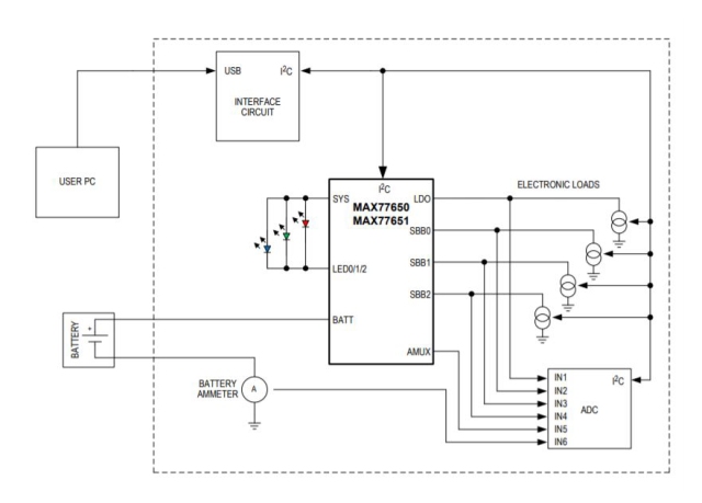
The MAX77650 and MAX77651 PMICs from Maxim Integrated include an integrated 150mA low-dropout regulator (LDO) that provides ripple rejection for noise-sensitive applications. A controller in the SIMO control scheme ensures that all outputs are attended to in a timely manner.
“Our customers in the field of wearables, hearables, and low-power IoT are at the intersection of high-end technology and aesthetics,” said Karthi Gopalan, product-line director for mobile power products at Maxim Integrated. “These markets are gaining massive traction with the increasing global dependence on smart AI assistants, on-the-go biometric tracking, and precision location tracking.”
Maxim Integrated’s low-power PMIC delivers “the highest system efficiency in the smallest form factor for such space-constrained designs,” she added. “Our PMIC can now slash solution size by half. This frees up board real estate to pack value-add modules such as voice commands, payment, GPS receivers, biometrics, gesture control, 3-D recognition, and camera modules.”
In automotive applications, the three primary challenges PMICs must manage are temperature, qualifications, and safety. Automotive applications require operation in an environment where the ambient temperature range is between –40°C and at least 105°C; therefore, any semiconductor devices used in automotive platforms must provide superior performance over a wider temperature range.
“Automotive applications require significantly higher quality levels to ensure near-zero failure rates during use extending beyond 10 years,” said Dialog’s Sandoval. “This has implications on the design, qualification requirements, and testing and screening of a device to ensure the highest quality levels can be met for the lifetime of the automobile.”
In the context of automotive applications, many elements of safety center on failure prevention. The device must have capabilities for managing electrical faults, providing for a possible resolution when they do occur. “Additional circuitry must be designed into the device to support this type of capability, resulting in higher complexity and cost,” said Sandoval.
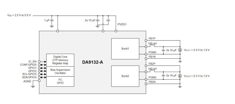
Dialog’s integrated DA913X-A devices enable a low system bill-of-materials cost and small solution footprint. The devices operate at efficiency levels in excess of 90%, reducing thermal design challenges for powering high-current rails in a range of systems, including ADAS.
The DA913X-A family consists of three devices, configured as single- or dual-output buck converters. The DA9130-A is a single-channel, two-phase buck converter that delivers up to 10 A of output current. The DA9131-A integrates two single-phase buck converters, each delivering up to 5 A of output. The DA9132-A also integrates two single-phase buck converters, each delivering up to 3 A. All three devices support input voltage of 2.5–5.5 V, with a 0.3- to 1.9-V output range, making them suitable for a variety of low-voltage systems. Output voltages above 1.9 V are supported by an external resistance divider.