
Considered science fiction just a couple of decades ago, self-driving vehicles are an emerging reality, made possible by the development of high-performance smart sensors. Technological progress in the digital and microcontroller spheres has made it possible to create sensors for lane keeping, adaptive cruise control, blind-spot detection, and other advanced driver assistance systems. ADAS features such as parking assist are both helpful tools for drivers and important solutions for meeting higher automotive safety standards. For example, the Euro NCAP Protocol, which regulates car safety standards in Europe and defines evaluation models, has mandated a set of ADAS safety features for inclusion in new vehicles.
LiDAR: What it is, how it works
Light detection and ranging (LiDAR), which uses electromagnetic radiation in the optical band for remote detection and measurement, is among the critical sensor technologies enabling ADAS. LiDAR is used today for pedestrian detection, blind spot detection, adaptive cruise control, and other applications that require detection and mapping of all the elements surrounding the vehicle.
LiDAR applies the same basic principle as radar but uses light pulses emitted by an infrared laser diode. By knowing the speed of the beam emitted, the moment of emission of the pulse, and the moment in which the reflected beam is detected, it is possible to calculate the distance of the object hit by the beam. This time-of-flight (ToF) technique is shown in Figure 1. The optical device has higher resolution than radar even at long distances and is thus able to obtain detailed three-dimensional images to aid in collision avoidance.
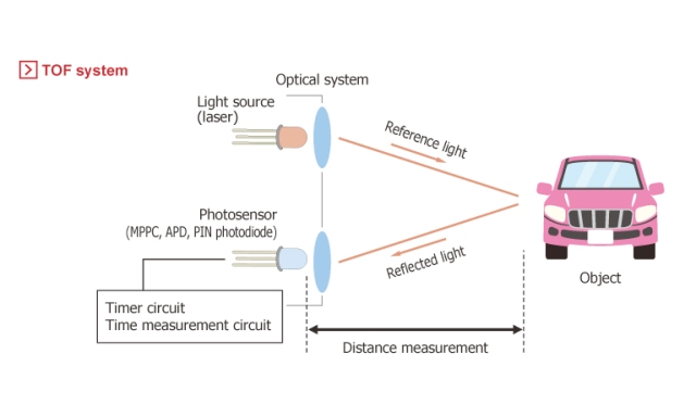
The principles behind LiDAR have been understood for decades, and the technology has found application in fields ranging from medical to military and now to automotive. But the use of a laser beam creates some important technological problems. If the laser is a high-resolution source, fully exploiting this characteristic to reconstruct the morphology of the environment in a detailed way through a scan requires high mechanical precision and a pulse speed on the order of nanoseconds. And while the electromagnetic waves used in radar systems have a fairly high reflection coefficient, this cannot be said for laser light; therefore, LiDAR requires higher energy. The laser light beams are generated by high currents (even on the order of tens of amperes) going through LED diodes; to avoid die overheating, the duty cycle must be low.
High pulse speed and higher energy lead to a very high power need from the electronic devices in the system, and as we all know, increasing the system power inevitably brings a host of technological challenges:
- Thermal management of power components and design of heat sinks
- Circuit energy efficiency
- Finding components that can handle the operating temperature
- Optimization of the board layout to minimize parasitic components
Inside the LiDAR: The laser driver
The LiDAR laser must be driven by a specially designed circuit capable of delivering a large amount of current in a very short time. The simplest driver consists of a component that acts as a current switch, in series with the laser.
One of the most used circuit topologies for the implementation of such a driver is the capacitor discharge resonant circuit, shown in Figure 2.
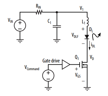
Q1 and DL are respectively the switch and the LED of the laser to be activated. If the switch is off, the C1 capacitor charges to the VIN voltage. When Q1 is turned on, C1 is discharged through DL and the L1 inductance, with which it forms a resonant circuit, so that the current flowing through the laser will be a sinusoidal pulse IDL, until the voltage across the LED is greater than its forward voltage. When the voltage on DL is less than VDLF, C1 starts charging again.
Charge time for this circuit is C1: tchr = RIN x C1, resonant discharge time is tres = 2 × π × √(L1 × C1), and equivalent impedance is R0 = √(L1⁄C1). If tchr is much larger than tres, then the RIN resistance has marginal effects on the L1-C1 resonator.
The advantages of this simple circuit are many:
- If known, parasitic inductances can be exploited.
- The waveform of the pulse is known.
- The energy transferred to the laser is in direct relationship with VIN: IDLpk = (VIN – VDLF) / R0.
- There is only one single-ended switching element, which is easy to control.
- The duration of the pulse transferred to the laser is shorter than the control on-time of the switching device.
In practice, though, the technological aspects of the circuit pose challenges: Given the high power involved, the switch must be a component with parasitic inductance close to zero and with ideally infinite switching speeds.
Classic silicon components, such as MOSFETs and JFETs, come up short in delivering the necessary features for implementation of a laser driver that can be used in automotive LiDAR systems. Higher power requires a larger MOSFET channel. That, in turn, lengthens the charging times of the parasitic capacitances, with consequent switching frequencies that are too low for the application. In addition, adequate thermal management would require bulky heat sinks. Using silicon components for the driver function requires the expertise of engineers and designers verse in high-power, high-frequency electronics.
GaN delivers the required parameters
The good news is that devices based on gallium nitride, a wide-bandgap material with an energy gap of 3.4 eV, have characteristics to satisfy the needs of automotive LiDAR systems. The electron mobility of GaN is hundreds of times greater than silicon’s, giving GaN devices the following advantages over their silicon counterparts:
- Lower RDS(on) activation resistance, which leads to lower conduction losses
- Lower parasitic capacitances, with a consequent decrease in losses during charging/discharging and therefore higher switching speeds
- Lower activation power requirements
- The ability to achieve the required characteristics in a smaller device with less overheating, lower board-space requirements, and a lower overall system cost
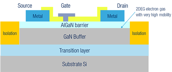
These characteristics satisfy the needs of the driver circuit switch component. Once the technology that is necessary for the implementation has been identified, we can analyze the characterization of the driver components.
Laser driver design considerations
Let’s start with the basic requirements for characterizing the circuit components, and then choose the GaN MOSFET devices suitable for the purpose. The basic parameters are the peak current flowing on the LED (IDLpk), the time width of the pulse (tw), the frequency of the pulses, and the voltage drop for the forward current on the LED (VDLF).
From the equation for equivalent impedance, considering that IDLpk = (VIN – VDLF) / R0, and setting the value of L1 (which for simplicity of circuit implementation must be as low as possible), we obtain C1 = L1 × (IDLpk / (VIN – VDLF))2. Since VIN = ((2 × π × L1) / (3tw)) × IDLpk VDLF, we get the IDLpk and VIN values needed to identify the GaN MOSFET device that best suits our design needs.
Further considerations center on the nature of the signals involved in the application, suggesting a design approach typical of RF circuits, and the construction materials of the boundary components such as resistance and capacitance of the charge-discharge resonant circuit.
Conclusions
The use of GaN components in commercial devices is only beginning. Technological solutions that were considered impossible or too complicated just a few years ago are proving to be successful in many areas, such as in power drivers for LiDAR systems. This confirms that, in the coming years, the field of power electronics, will be dominated by WBG devices, which are able to solve the technological limits of their silicon-based predecessors.