
Professor Yue Zhao and his PESLA team have been leading the effort in developing silicon carbide–based power converters from several kilowatts to the megawatts for future transportation electrification and grid-tied applications.
The Power Electronic System Laboratory at Arkansas (PESLA) is a key part of the University of Arkansas Power Group’s research into the development of next-generation power electronic systems with improved power density, efficiency, and reliability. Professor Yue Zhao and his PESLA team have been leading the effort in developing silicon carbide–based power converters from several kilowatts to the megawatts for future transportation electrification and grid-tied applications.
While SiC power devices offer improved efficiency and power density compared with their Si counterparts, challenges remain in the gate control due to potential excessive voltage overshoot and noise that can be induced by the fast switching that these devices allow. High dV/dt and di/dt during switch-on and -off transients can result in system instability, reliability issues, and device failure. To address this, digital gate drivers (DGDs) for SiC MOSFETs are a focus of active development. Compared with conventional analog gate drivers used to drive Si with fine-tuned external gate resistance (RG) (resistors RGon and RGoff in the turn-on/turn-off gate drive paths would be tuned), DGDs offer user-defined flexibility and tradeoff between converter efficiency and switching performance.1
In this article, we will share work done by PESLA on a 75-kW grid-tied inverter2 with a 1-kV DC-link voltage and a 480-Vrms line-to-line output voltage using the SiC half-bridge power module MSCM170AM058CD-3AG rated at 1.7 kV and 281 A at 80˚C. The DGD is based on Microchip Technology’s patented Augmented Switching scheme.
As shown in Figure 1, the Augmented Turn-Off (ATOff) used in this case consists of a user-defined gate voltage (Vgs) level and a time interval, designated in the figure as ATOff Level and ATOff Time. Under normal operation, these parameters control the turn-off transition of the FET by using a two-level (2L) turn-off, allowing the Miller plateau period to be extended, thereby slowing the dV/dt and di/dt transitions and hence lowering drain voltage (Vds) overshoots. Compare this with the analog approach shown, where this would be done in a less effective way by changing the values of RGoff on the gate driver hardware. The DGD hence allows removal of Miller clamp circuits typically used with analog gate drivers. As shown in Figure 1, under fault conditions, Augmented Switching allows further control on the turn-off transients and potentially catastrophic avalanche conditions can hence be avoided, for example, by coupling these ATOff transition steps with a smaller external RGoff.
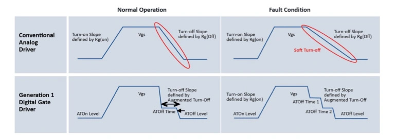
The DGD core 2ASC-17A1HP offered by Microchip Technology offers a resolution of 0.25 V and 32 ns, respectively, for the ATOff Level and ATOff Time.
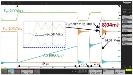
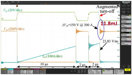
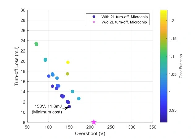
Figures 2a and 2b show the turn-off transition on the SiC module switching at 1 kV and 300 A when using the DGD. Figure 2a is when the 2L turn-off is disabled, while Figure 2b shows this with optimized settings for the 2L turn-off. These optimized settings were found using double-pulse testing. As seen from Figure 2, the DGD can reduce the Vds overshoot from 209 V to 150 V and dV/dt from 34.51 V/ns to 23.83 V/ns, while increasing switching loss Eoff from 8.04 mJ to 11.8 mJ.
The PESLA group has come up with a cost function J defined as
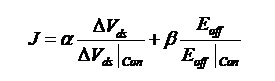
where ∆Vds and Eoff are thevoltage overshoot and turn-off switching loss at each test with Augmented Turn-Off enabled, and ∆Vds|con and Eoff|conare the overshoot and turn-off loss with Augmented Turn-Off disabled. α and β are weighing factors that satisfy α β = 1. The user can adjust the values of α and β based on their application requirements to address the tradeoff between the voltage overshoot reduction and the increase of switching loss.
Figure 3 shows the flexibility that DGD offers, enabling users in this case to trade off switching loss with the Vds overshoot. The minimum cost point showing the optimal tradeoff with DGD is shown in this figure.
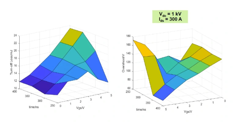
With two independent variables, ATOff Time and ATOff Level, a 3D map can be created showing the effect of the variation of these parameters on switching loss and performance such as Vds overshoot. The PESLA group conducted such studies3 on the Microchip Technology MSCSM170AM058CT6LIAG, which is a 1.7-kV SiC MOSFET phase-leg power module. In this experiment, the DC bus voltage is 1 kV, the air core inductor is 40 µH, and the module is turning off a 300-A load current. Figure 4 shows the 3D map on this module for the Eoff and ∆Vds overshoot as the ATOff time and ATOff Level is varied. A user can therefore choose the tradeoff in these parameters based on the end-use application. In addition, PESLA has demonstrated the effectiveness of the DGD on other SiC module platforms, such as a module from Cree Wolfspeed.4
The poorer short-circuit withstand time in SiC MOSFETs (compared with Si) requires the gate driver to include real-time protection features from fault conditions like power supply undervoltage and overvoltage lockout, desaturation detection, and temperature monitoring with a fast response time to prevent catastrophic device and/or system failure. More complex gate drivers are being developed for SiC power modules that include real-time (~1-ns) resolution for load current and functional safety.5 As device power densities and/or slew rates increase, these will be increasingly fundamental to the end application use.
“The digital gate driver is an essential tool to investigate the switching performance of SiC power modules,” said Zhao. “It is smart and enables lots of possibilities without the need for soldering irons. It has the potential to unleash the power of SiC devices at the converter level while addressing the challenges brought by them.”
References
1Zhao et al. (Feb. 2020). “Adaptive Multi-Level Active Gate Drivers for SiC Power Devices.” IEEE Transactions on Power Electronics.
2Wu et al. (2022). “Design and Demonstration of A 75 kW Grid-Tied Inverter using Low-Inductance 1.7 kV Silicon Carbide Modules.” PCIM 2022.
3Diao et al. (2022). “Design and Performance Assessment of a Digital Gate Driving Solution for Silicon Carbide Power Modules.” PCIM 2022.
4Diao et al. (2022). “A Modular and Performance-Tunable Silicon Carbide Half-Bridge Building Block with Digital Gate Driver.” 2022 IEEE Applied Power Electronics Conference and Exposition (APEC), pp. 251–258, doi: 10.1109/APEC43599.2022.9773504.
5Kawai et al. (2021). “A 1ns-Resolution Load Adaptive Digital Gate Driver IC with Integrated 500 ksps ADC for Drive Pattern Selection and Functional Safety Targeting Dependable SiC Application.” 2021 IEEE ECCE Conference.