
Producing a top quality ATE PCB requires design experience and savvy design techniques to assure chip testers achieve the highest accuracy.
“Load boards” was the term used in the semiconductor industry for automated test equipment (ATE) PCBs a few years back. However, in recent years, they’ve been referred to as “device interface boards (DIBs)” or “handler interface boards (HIBs)” in the semiconductor industry. Chipmakers evaluating their newly minted and highly advanced products need quick turn and high quality when ordering test boards, regardless of the brand. This is more than what was required for past generations of test boards.
This is because chip fabrication speeds are far faster now than they were a few years ago. Chipmakers are keen to test their goods as quickly as feasible because they are generating them at a faster rate. Fabrication timeframes used to be two to three months, but today they’re closer to six to eight weeks. Chip manufacturers require their ATE PCB boards as soon as possible in order to test their new chips, and they don’t want millions of dollars’ worth of chips lying about idly.
ATE PCB providers had two to three months to deliver these test boards back in the day. However, they now have six to eight weeks to turn around an ATE PCB, which is required by chipmakers. ATE PCB providers may sweeten the offer by including other services. Chipmakers, for example, gain a bonus when an electronics manufacturing services (EMS) supplier, such as Naprotek, provides wafer testing and inspection, handling, dicing, and semiconductor packaging in addition to the ATM test board.
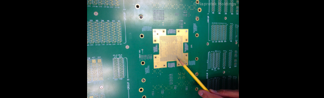
To provide high-quality ATE PCBs (Fig. 1), design knowledge and intelligent design methodologies are required.
This includes having a fine touch and precise knowledge of place and route associated with the design of these large boards, as well as understanding all the nuances associated with shrinking ball-grid array (BGA) packaging, dramatically reduced pitch between BGA balls, and having a fine touch and precise knowledge of place and route associated with the design of these large boards.

Quality and Accuracy
A well-designed and accurate ATE PCB is the result of a variety of design methodologies, policies, and procedures. For example, assurances must be established on the placement of bypass capacitors and the presence of voltage constraints.
Others, well beyond those connected with a standard multi-layer board, exist since the designer is now constructing a 30 to 50-layer board. A high-quality ATE test board is created through focused design procedures and adheres to tight fabrication criteria.
Otherwise, the accuracy of the test board results will be compromised. One with a high fail rate, for example, is likely to be inaccurate. You’re throwing away decent chips and a lot of money when you do this. As a result, here is where quality comes into play.
Here are some of the first measures taken by an experienced ATE PCB designer to ensure quality and accuracy. To begin, they must evaluate the fact that today’s ATE PCB is densely loaded with BGAs. As the size of this device packaging continues to diminish, that packaging technology has become dynamic. Not only is the BGA shrinking, but the pin pitch between BGA balls is shrinking as well.
Five years ago, BGA pitch was at 1.0 or 0.8 millimeter (mm). Today, it is at 0.25 to 0.3mm. That dramatic reduction in pin pitch translates into challenging design constraints during PCB layout. Tighter pitches and smaller BGAs are therefore one aspect that an experienced ATE PCB designer has to take into account.
Also consider that trace widths have become narrower. Two to three years ago, trace widths were seven to eight mils. Today, they’ve shrunk down to three to four mils.
Given these technology advances, the ATE PCB designer has to have enough experience to figure out proper place and route. For example, the designer is using a 0.3mm pitch BGA. Routing that BGA cannot fan out with a very wide trace. Instead, three to four mil traces must be used. The previous technique was that when traces were brought out of the BGA, they were brought out at a different width. After a trace came out, the designer would increase the width.
But take a 2.5 or 3.0 mil trace coming out of today’s BGA as an example. The designer cannot drastically increase that trace to seven or eight mils. The result would be considerable signal loss or change in the speed or the impedance based on the changing widths. Therefore, the savvy designer needs to take that into account while working on routing and selecting differential pair widths or high-speed traces.
A particular stackup is required for differential pairs. Those differential pairs are designed based on the chipmaker’s requirements. When the ATE board is fabricated, the fab shop needs to assure that differential pairs are correctly impedance matched and that those differential pairs are at 5% tolerance.
For example, if differential pairs are 100 ohms (Ω) impedance matched, the designer is allowing a 5% tolerance, meaning that tolerance would fall between 95 and 105 Ω. If differential pairs are not properly matched based on the impedance the ATE PCB designer provides the fabricator, chip test results will not be as accurate as required.
Focus on the DUT
Above all, considerable design attention goes to the device-under-test or DUT area of the ATE PCB, as shown in Figure 2. After assuring the early stages of a design are correct, the designer places careful attention on a trio of main design considerations – high-speed traces, curve routing, and length matching.
The chipmaker provides data for the high-speed traces. That’s usually in the schematic or specification sheet. It includes the number of high-speed traces in the design and designates the ones that are serial/de-serializer (SerDes), loop back, and SerDes with capacitors. As shown in Figure 3, loop back traces go from and to the pin of the DUT, typically a BGA package. These traces are typically routed close to each other and are approximately equal in length for them to function optimally.
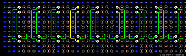
Figure 4 shows SerDes routing. For the high-speed SerDes trace, the via pattern is placed close to the socket so that the trace coming from the BGA to the via and then again from the via to the BGA pin. High-speed signals are transmitted from the BGA pins to via pattern and then again from via pattern to different BGA pins, for transmission and reception of the signals, respectively.

The third type of high-speed trace involves routing SerDes with capacitor. The trace routing is terminated on the two pins of the two capacitors. Then, traces are routed again back to the BGA pin.
Lesser value and smaller capacitors are placed on the BGA because they have a faster response time. They are placed on top and close to the BGA pins, allowing them to start their functions very fast. Traditionally, placing the 0201 capacitors as close to and on the socket pins allow the transmission of signals to maintain their high speeds.
At Assembly
Quality and accuracy then follow design into the PCB assembly floor. Some leading EMS providers provide chipmakers what’s known as factory purpose built for quality. For example, Naprotek has on its assembly line several distinct quality and inspection stages throughout the flow of the ATE test board. All PCBs, including ATE test boards, are assembled and manufactured according to the highest IPC Class 3 Quality Standards.
For low quantity boards numbering 10 or below, the inspection stages—across the process include — solder paste inspection, first article quality control (FA QC), and surface mount quality control (SMT QC). First article refers to the initially produced board, also known as the “golden board.”
The first step is printing solder paste on the board and performing solder paste inspection to assure solder deposit is adequate. Then, once components are placed on an un-reflowed board, it undergoes FAQC, which checks the polarity and values of the components. Thirdly, once FAQC passes, the board goes through reflow. Once that’s done, the first article board undergoes SMT QC. At this point, a 100% visual inspection is performed to determine solder joint quality and check for defects.
For high quantity boards going beyond 10, for instance, 15 or 20, quality and inspection stages are virtually the same as for low quantity test boards. However, another inspection stage is included after SMT QC. This is called automated optical inspection or AOI. At this stage, an AOI program is generated. Then, all boards coming out of SMT are inspected based on that AOI program. When the boards move from SMT to THT (Through-hole Technology), all boards go through TH loading and selective soldering. Once all THT components are soldered, X-ray inspection is done on TH components to determine barrel fill and voiding percentages. Profile specifications are tweaked at each process step to get the best results on the board.
Looking Out in Time
As we’ve said here, technologies supporting high quality and highly accurate ATE PCBs are rapidly advancing. Given that BGA packaging continues to become smaller, there is a point out in time, perhaps two to three years, when microelectronics design and assembly will need to be ushered in to create hybrid SMT and microelectronics-based test boards. Chipmakers are no strangers to such technologies as flip chips and multi-tier wire bonding become more and more prevalent in microelectronics assembly. Therefore, semiconductor engineering managements assigned to perform testing duties need to collaborate with their ATE PCB providers to fully understand how they can be successful with future chip test boards.